Display panel and preparation method thereof

A display panel and via technology, which is applied in semiconductor/solid-state device manufacturing, electrical components, electric solid-state devices, etc., can solve the problems of high cost, poor stability and reliability of GSD structure devices, etc., to reduce contact resistance and improve stability performance and reliability, and the effect of improving thermal oxidation problems

Pending Publication Date: 2021-02-26
SHENZHEN CHINA STAR OPTOELECTRONICS SEMICON DISPLAY TECH CO LTD
View PDF6 Cites 9 Cited by
  • Summary
  • Abstract
  • Description
  • Claims
  • Application Information

AI Technical Summary

Problems solved by technology

[0004] An embodiment of the present invention provides a display panel, which is used to solve the technical problems of high cost of the top gate structure backplane in the prior art, or poor stability and reliability of GSD structure devices

Method used


Image

  • Display panel and preparation method thereof
  • Display panel and preparation method thereof
  • Display panel and preparation method thereof

Examples


Embodiment Construction

[0020] The following will clearly and completely describe the technical solutions in the embodiments of the present invention with reference to the drawings in the embodiments of the present invention. In the drawings, for clarity and ease of understanding and description, the size and thickness of the components shown in the drawings are not in scale.

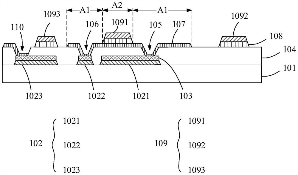
[0021] like figure 1 As shown, in the basic structural diagram of the display panel provided by the embodiment of the present invention, the display panel includes: a substrate layer 101, a first metal layer 102, a thermal oxidation protection layer 103, a buffer layer 104, an active layer 107, a gate an insulating layer 108 , and a second metal layer 109 . The first metal layer 102 is located on the substrate layer 101 and includes a source 1021 and a drain 1022 . The thermal oxidation protection layer 103 is located on the first metal layer 102 . The buffer layer 104 is located on the substrate layer 101 and covers the th...


PUM

PropertyMeasurementUnit
thicknessaaaaaaaaaa
thicknessaaaaaaaaaa
thicknessaaaaaaaaaa

Abstract

The invention provides a display panel and a preparation method thereof. The display panel comprises a substrate layer, a first metal layer located on the substrate layer, a thermal oxidation protection layer located on the first metal layer, a buffer layer located on the substrate layer and covering the thermal oxidation protection layer, an active layer located on the buffer layer, a gate insulating layer positioned on the active layer and the buffer layer, and a second metal layer positioned on the gate insulating layer, wherein the first metal layer comprises a source electrode and a drainelectrode, and the second metal layer comprises a grid electrode and a grid line. According to the invention, the source / drain electrode of a thin film transistor is arranged on the surface of the substrate layer, so shading effect is achieved, and the frequency of a yellow light process is reduced.

Description

technical field [0001] The invention relates to the field of display technology, in particular to a display panel and a preparation method thereof. Background technique [0002] Mini / Micro LED (MLED) display technology has entered a stage of rapid development in the past two years. Compared with OLED display panels, MLED display panels show better performance in terms of cost, contrast, high brightness and thin and light appearance. In MLED display technology, the backplane technology is particularly critical. The backplane of the top gate structure consists of three layers of metal to form a sandwich structure, which can obtain greater capacitance in a smaller space. However, the current MLED top-gate structure backplane technology usually requires 10 mask processes, which is costly and unfavorable for the mass production of MLED display technology. [0003] In the existing technology, the gate, source, and drain are prepared on the same layer and patterned together. Altho...

Claims


Application Information

Patent Timeline
Patent Type & Authority Applications(China)
IPC IPC(8): H01L27/12H01L27/15H01L33/48H01L33/62H01L21/77
CPCH01L27/1225H01L27/1237H01L27/127H01L27/1288H01L33/48H01L33/62H01L27/156H01L2933/0033H01L2933/0066
Inventor 罗传宝卢马才
Owner SHENZHEN CHINA STAR OPTOELECTRONICS SEMICON DISPLAY TECH CO LTD
Why Eureka
Try Eureka