Solder ball arrangement unit and packaging chip

A technology of solder balls and chips, which is applied in the direction of electrical components, semiconductor/solid-state device parts, semiconductor devices, etc., can solve the problems of crosstalk deterioration, shorten the physical distance of the receiving port, expand the chip area, etc., and increase the signal transmission speed , The effect of increased solder ball density and small chip area

Active Publication Date: 2021-02-26
SHENZHEN PANGO MICROSYST CO LTD
View PDF9 Cites 0 Cited by
  • Summary
  • Abstract
  • Description
  • Claims
  • Application Information

AI Technical Summary

Problems solved by technology

[0004] The TXP and TXN and RXP and RXN between the serializer channels of the above-mentioned existing technical solutions are arranged in parallel, and the crosstalk is large, but if the distance is opened according to the existing method of increasing the isolated ground solder balls, the chip area will be enlarged
This makes the integrated chip unable to achieve miniaturization. However, if the small-pitch solder ball arrangement is used, the channel physical distance between the receiving port (TX) and the transmitting port (RX) will be shortened, and the crosstalk will deteriorate.

Method used


Image

  • Solder ball arrangement unit and packaging chip
  • Solder ball arrangement unit and packaging chip
  • Solder ball arrangement unit and packaging chip

Examples


Embodiment 1

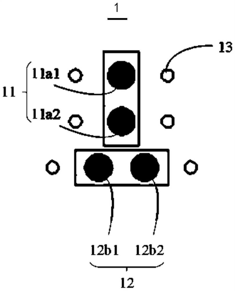
[0038] see image 3 , image 3is a schematic diagram of the first structure of the solder ball arrangement unit in the embodiment of the present invention. The solder ball arrangement unit 1 includes a first signal solder ball pair 11, a second signal solder ball pair 12, and 6 ground solder balls surrounding the first signal solder balls 11a1 and 11a2 and the second signal solder balls 12b1 and 12b2 13. In the embodiment of the present invention, the first pair of signal solder balls 11 and the second pair of signal solder balls 12 are vertically arranged to form an inverted T shape, and six ground solder balls 13 are separately arranged on the first pair of signal solder balls 11 and the second pair of signal solder balls. The two signal solder ball pairs are arranged symmetrically on both sides of the 12 . Specifically, in the vertical first direction, three rows are respectively arranged at intervals, a grounding ball c is symmetrically arranged on both sides of the fir...

Embodiment 2

[0040] see Figure 4 , Figure 4 is a schematic diagram of the second structure of the solder ball arrangement unit in the embodiment of the present invention. The solder ball arrangement unit 1 includes a first signal solder ball pair 11, a second signal solder ball pair 12, and 9 ground solder balls surrounding the first signal solder balls 11a1 and 11a2 and the second signal solder balls 12b1 and 12b2 13. In the embodiment of the present invention, the first pair of signal solder balls 11 and the second pair of signal solder balls 12 are vertically arranged to form an inverted T shape, and nine ground solder balls 13 are separately arranged on the first pair of signal solder balls 11 and the second pair of signal solder balls. Both sides of the two signal solder ball pairs 12 and between the first signal solder ball pair 11 and the second signal solder ball pair 12 are arranged symmetrically. Specifically, in the vertical first direction, a ground solder ball c is symmet...


PUM


Abstract

The invention provides a solder ball arrangement unit and a packaging chip. The solder ball arrangement unit comprises a first signal solder ball pair and a second signal solder ball pair which are vertically arranged, and a plurality of grounding solder balls disposed around the first signal solder ball pair and the second signal solder ball pair, wherein the first signal solder ball pair comprises two first signal solder balls arranged at an interval along a first direction, the second signal solder ball pair comprises two second signal solder balls arranged at an interval along a directionvertical to the first direction, and the projections of the first signal solder balls along the first direction fall into the interval between the two second differential signal solder balls. Throughthe above mode, the crosstalk between the solder ball arrangement units in the packaged chip is small, the signal transmission speed is increased, the solder ball density in the prepared chip is improved, the chip area is small, and the preparation of a microchip is facilitated.

Description

technical field [0001] The invention relates to the technical field of packaging, in particular to a solder ball arrangement unit and a packaged chip. Background technique [0002] As the connection carrier between the silicon chip and the PCB, the package plays the role of signal transmission and is an important part of the chip. With the development of serial communication technology, the single channel rate has reached 112Gbps; and the system capacity is getting larger and larger, it is inevitable to integrate multiple serial channels in a single chip. Multiple high-speed serial channels are transmitted in the package, and there will be a problem of crosstalk between channels. [0003] At present, the main solder ball arrangement methods in the industry are as follows: figure 1 and figure 2 :in figure 1 and figure 2 TXP is the positive receiving port, TXN is the negative receiving port, RXP is the positive transmitting port, RXN is the negative transmitting port, a...

Claims


Application Information

Patent Timeline
IPC IPC(8): H01L23/488
CPCH01L24/14H01L2224/14134
Inventor 班荣兴梁远军
Owner SHENZHEN PANGO MICROSYST CO LTD
Why Eureka
Try Eureka