
Method for positioning failure point in semiconductor device

A positioning method and failure point technology, applied in semiconductor/solid-state device testing/measurement, electrical components, circuits, etc., can solve problems such as inability to locate, and achieve the effect of simple and effective positioning

Active Publication Date: 2021-02-26
HUA HONG SEMICON WUXI LTD
View PDF4 Cites 0 Cited by
  • Summary
  • Abstract
  • Description
  • Claims
  • Application Information

AI Technical Summary

Problems solved by technology

[0004] However, in failure analysis, it sometimes happens that the FIB (Foucs ion beam, focused ion beam) machine does VC (Voltage Contrast, voltage comparison test) and cannot locate the failure point

Method used


Image

  • Method for positioning failure point in semiconductor device
  • Method for positioning failure point in semiconductor device
  • Method for positioning failure point in semiconductor device

Examples


Embodiment Construction

[0031] The technical solutions in this application will be clearly and completely described below in conjunction with the accompanying drawings. Apparently, the described embodiments are part of the embodiments of this application, not all of them. Based on the embodiments in this application, all other embodiments obtained by persons of ordinary skill in the art without making creative efforts belong to the scope of protection of this application.

[0032] In the description of this application, it should be noted that the terms "center", "upper", "lower", "left", "right", "vertical", "horizontal", "inner", "outer" etc. The indicated orientation or positional relationship is based on the orientation or positional relationship shown in the drawings, and is only for the convenience of describing the present application and simplifying the description, rather than indicating or implying that the referred device or element must have a specific orientation, use a specific orientati...


PUM


Abstract

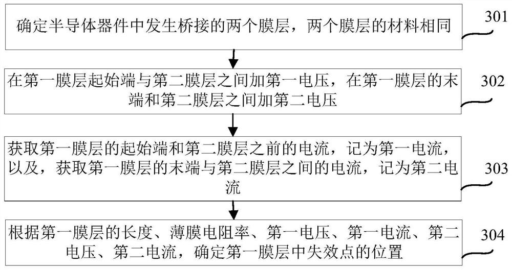
The invention discloses a method for positioning a failure point in a semiconductor device, and relates to the field of semiconductor manufacturing. The method for positioning the failure point in thesemiconductor device comprises the following steps of determining two film layers which are bridged in the semiconductor device, wherein the two film layers are made of the same material; applying afirst voltage between the starting end of the first film layer and a second film layer, and applying a second voltage between the tail end of the first film layer and the second film layer; obtaininga current between the starting end of the first film layer and the second film layer, and recording the current as a first current, and obtaining a current between the tail end of the first film layerand the second film layer, and recording the current as a second current; and determining the position of the failure point in the first film layer according to the length of the first film layer, the film resistivity, the first voltage, the first current, the second voltage and the second current. A problem that the failure point cannot be positioned through a VC method of an FIB machine table in current failure analysis is solved. And the effect of simply, conveniently and effectively positioning the failure point is achieved.

Description

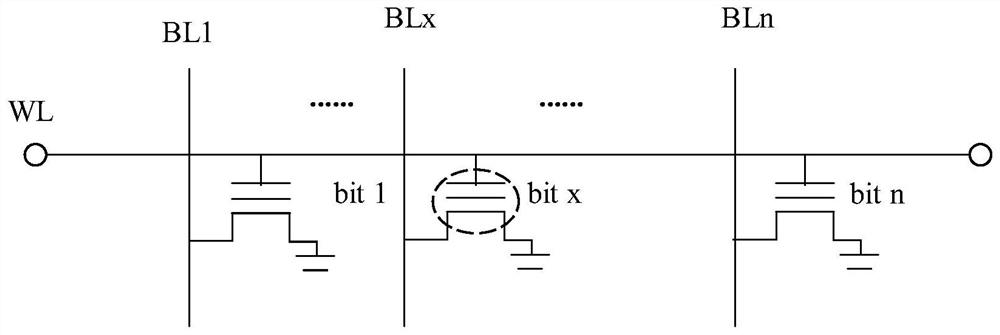
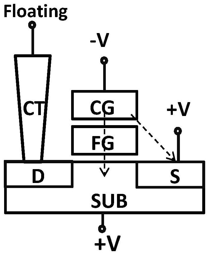
technical field [0001] The present application relates to the field of semiconductor manufacturing, in particular to a method for locating failure points in semiconductor devices. Background technique [0002] In the production process of semiconductor devices, failure analysis is an important process to improve and enhance the quality of semiconductor devices. Failure analysis includes external inspection, non-destructive analysis, electrical performance testing, destructive analysis, etc. [0003] In the electrical performance test of Nor flash, the stress test of the probe test will be carried out. For example, a voltage is added to the word line of the Nor flash, and another voltage is added to the source and the substrate to test the device. pressure performance. Such as figure 1 As shown, in the structure of Nor flash, n bits in the same row are controlled by a word line WL, and bits in the same column are controlled by a bit line BL. If any bit breaks down in the ...

Claims


Application Information

Patent Timeline
Patent Type & Authority Applications(China)
IPC IPC(8): H01L21/66
CPCH01L22/14H01L22/26
Inventor 苏凤梅
Owner HUA HONG SEMICON WUXI LTD
Learn More