Display panel, manufacturing method thereof and display device

A display panel and liquid crystal panel technology, applied in the field of display panels and display devices, can solve the problems of decreased touch accuracy and sensitivity of display panels, crosstalk of touch sensor signals, etc., to improve accuracy and sensitivity, increase distance, The effect of reducing the influence of signal crosstalk

Active Publication Date: 2021-02-26
SHENZHEN CHINA STAR OPTOELECTRONICS SEMICON DISPLAY TECH CO LTD
View PDF9 Cites 1 Cited by
  • Summary
  • Abstract
  • Description
  • Claims
  • Application Information

AI Technical Summary

Problems solved by technology

[0005] Embodiments of the present application provide a display panel, a manufacturing method thereof, and a display device, which are used to solve the problem of signal crosstalk between the light control sensor and the touch sensor in the existing display panel integrating light control sensors and touch sensors, which causes the display panel to touch. The accuracy and sensitivity of the control are reduced

Method used


Image

  • Display panel, manufacturing method thereof and display device
  • Display panel, manufacturing method thereof and display device
  • Display panel, manufacturing method thereof and display device

Examples


Embodiment Construction

[0029] The following descriptions of the various embodiments refer to the accompanying drawings to illustrate specific embodiments that the present application can be used to implement. The directional terms mentioned in this application, such as [top], [bottom], [front], [back], [left], [right], [inside], [outside], [side], etc., are for reference only The orientation of the attached schema. Therefore, the directional terms used are used to illustrate and understand the application, but not to limit the application. In the figures, structurally similar elements are denoted by the same reference numerals.

[0030] The present application will be further described below in conjunction with the accompanying drawings and specific embodiments.

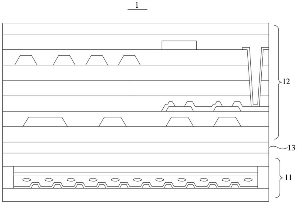
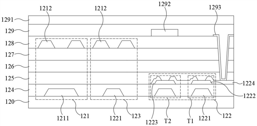
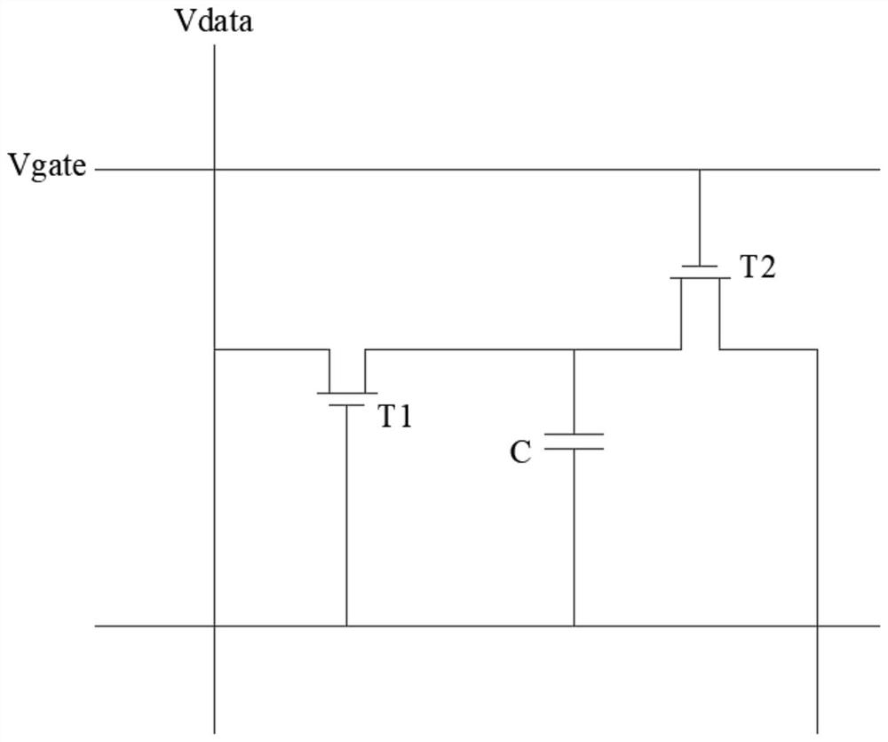
[0031] The embodiment of the present application provides a display panel, which is combined with Figure 1 to Figure 3 For details, figure 1 A schematic structural diagram of a display panel provided in an embodiment of the present ap...


PUM

PropertyMeasurementUnit
thicknessaaaaaaaaaa

Abstract

The invention provides a display panel, a manufacturing method thereof and a display device. The display panel comprises a liquid crystal panel and a touch panel arranged on the liquid crystal panel,and the touch panel comprises a substrate and a plurality of touch sensors and light-operated sensors which are alternately arranged on the substrate in an array mode; each touch sensor is composed ofa plurality of columns of transmitting electrodes arranged at intervals in the first direction and a plurality of columns of receiving electrodes arranged at intervals in the direction perpendicularto the first direction, and each light-operated sensor comprises a plurality of gate electrodes arranged in an array mode. A first transparent organic film layer with a low dielectric constant is arranged between each receiving electrode of each touch sensor and each gate electrode of each light-operated sensor which are arranged in a layered manner, so that the distance between the receiving electrodes and the gate electrodes is increased, and the parasitic capacitance between the receiving electrodes and the gate electrodes is reduced; the influence of the light-operated sensors on the signal crosstalk of the touch sensors is reduced, and the touch accuracy and sensitivity of the display panel integrated with the light-operated sensors and the touch sensors are improved.

Description

technical field [0001] The present invention relates to the field of display technology, in particular to a display panel, a manufacturing method thereof, and a display device. Background technique [0002] With the development of display technology, it is also a trend to integrate sensors into display panels. The touch and light sensors currently used are to attach the sensor to the outside of the display panel, which will not only reduce the light transmittance of the display panel, but also increase the manufacturing cost, while integrating the sensor in the display panel can effectively reduce the The loss of light can also reduce manufacturing costs. [0003] In the existing display panels that synchronously integrate the light control sensor and the touch sensor, the touch sensor is usually a mutual capacitance structure, which is composed of multiple rows of emitting electrodes arranged horizontally and multiple columns of receiving electrodes arranged vertically, an...

Claims


Application Information

Patent Timeline
Patent Type & Authority Applications(China)
IPC IPC(8): G02F1/1333G02F1/1368G02F1/1362
CPCG02F1/13338G02F1/1368G02F1/136213
Inventor 查宝江淼姚江波陈黎暄张鑫
Owner SHENZHEN CHINA STAR OPTOELECTRONICS SEMICON DISPLAY TECH CO LTD
Why Eureka
Try Eureka