


Quick Research
Generate reliable direction feasibility study reports for your R&D in just a few steps.

Technical Q&A
Discover and master advanced knowledge NOW. Basics, ideas, possibilities, all at once.

Find Solutions
As an expert in R&D theories, this can generate solutions to your technical problems instantly.

Evaluate Feasibility
Analyze your overall solution with one click, know your potential R&D risks in advance.

Monitor Landscape
Get weekly tech updates, stay abreast of the latest tech innovations and key insights.
optical module
An optical module and optical interface technology, applied in the field of optical modules, can solve problems such as module failure, chip performance degradation, failure, etc., to reduce the impact of signal crosstalk, efficient heat dissipation, and increase the distance.
- Summary
- Abstract
- Description
- Claims
- Application Information
AI Technical Summary
Problems solved by technology
Method used
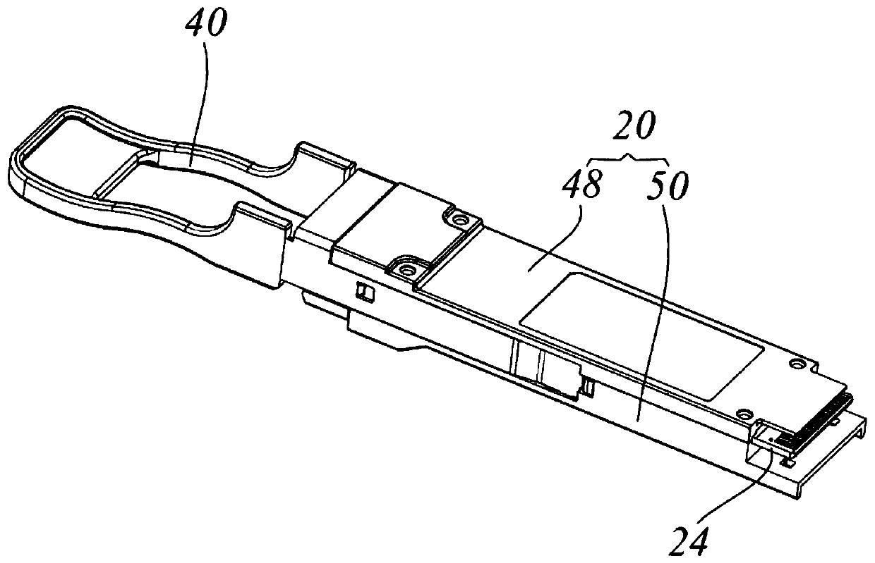
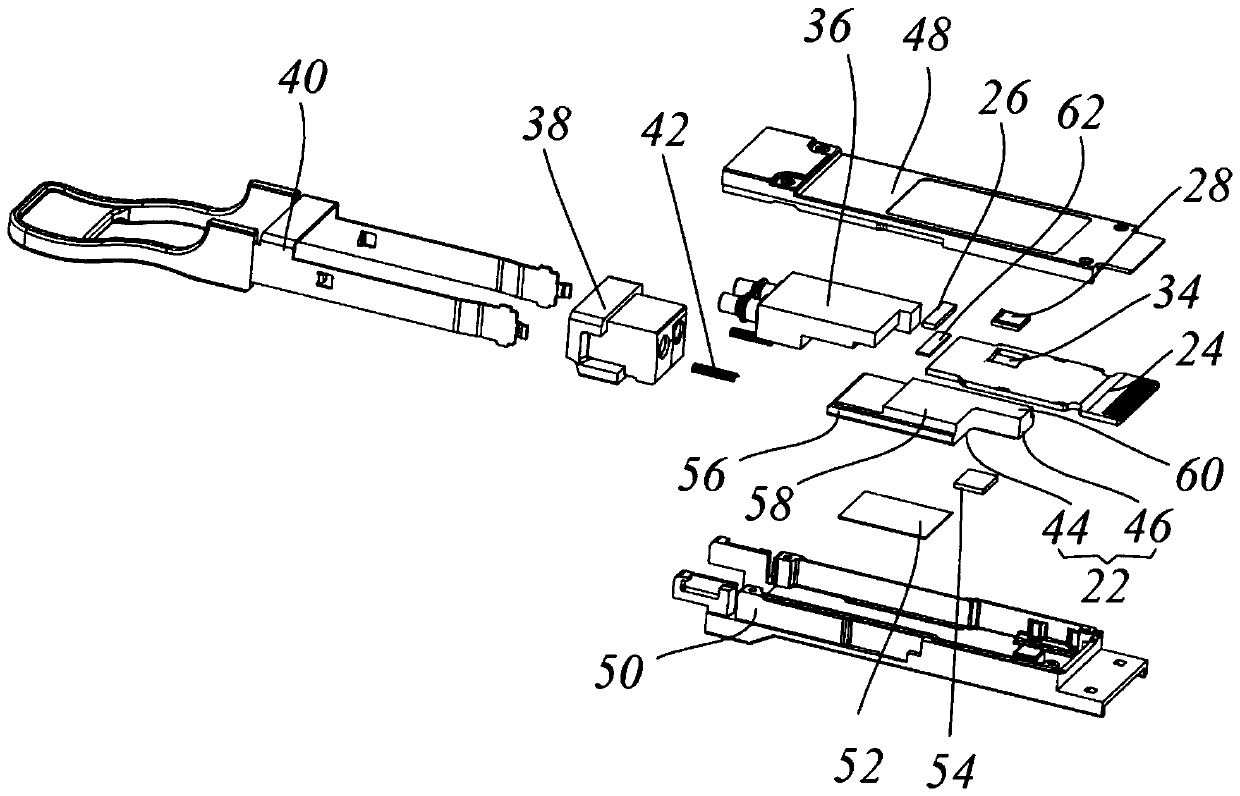
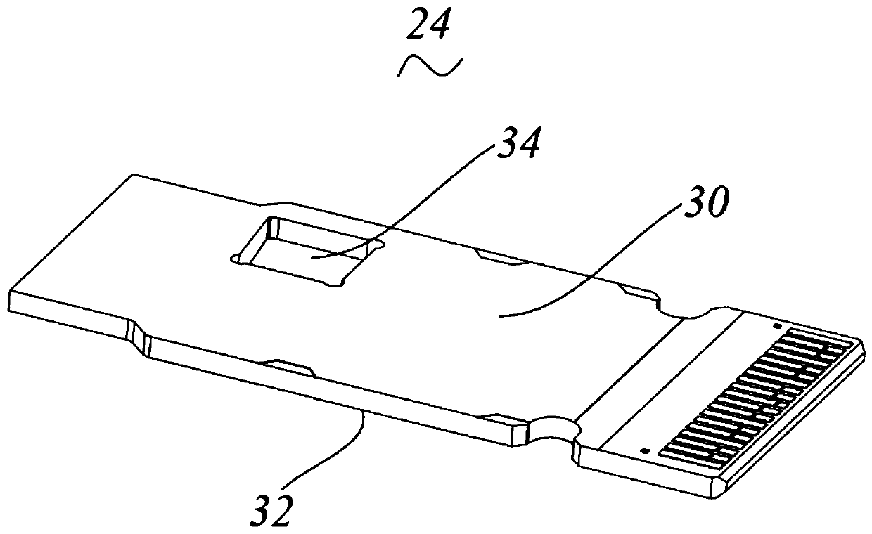
Image

Examples
Embodiment Construction
[0033] The application will be described in detail below in conjunction with specific implementations shown in the accompanying drawings. However, these implementations do not limit the present application, and any structural, method, or functional changes made by those skilled in the art based on these implementations are included in the protection scope of the present application.
[0034] In each drawing of the present application, some dimensions of structures or parts are exaggerated relative to other structures or parts for convenience of illustration, and therefore, are only used to illustrate the basic structure of the subject matter of the present application.
[0035] In addition, terms used herein such as "upper", "above", "under", "below", etc. to express relative positions in space are for convenience of description to describe a unit or feature as shown in the drawings relative to A relationship to another cell or feature. The terms of spatial relative position ...
PUM
 Abstract
Description
Claims
Application Information
 - R&D Engineer
- R&D Manager
- IP Professional
- Industry Leading Data Capabilities
- Powerful AI technology
- Patent DNA Extraction
Browse by: Latest US Patents, China's latest patents, Technical Efficacy Thesaurus, Application Domain, Technology Topic, Popular Technical Reports.
© 2024 PatSnap. All rights reserved.Legal|Privacy policy|Modern Slavery Act Transparency Statement|Sitemap|About US| Contact US: help@patsnap.com