Low-cost high-efficiency solar cell and preparation method thereof
A solar cell, low-cost technology, applied in the field of solar cells, can solve the problems of thick polysilicon film, affect passivation performance, low content, etc., achieve the effects of good conductivity, ensure passivation, and reduce passivation loss
- Summary
- Abstract
- Description
- Claims
- Application Information
AI Technical Summary
Problems solved by technology
Method used
Image
Examples
Embodiment 1
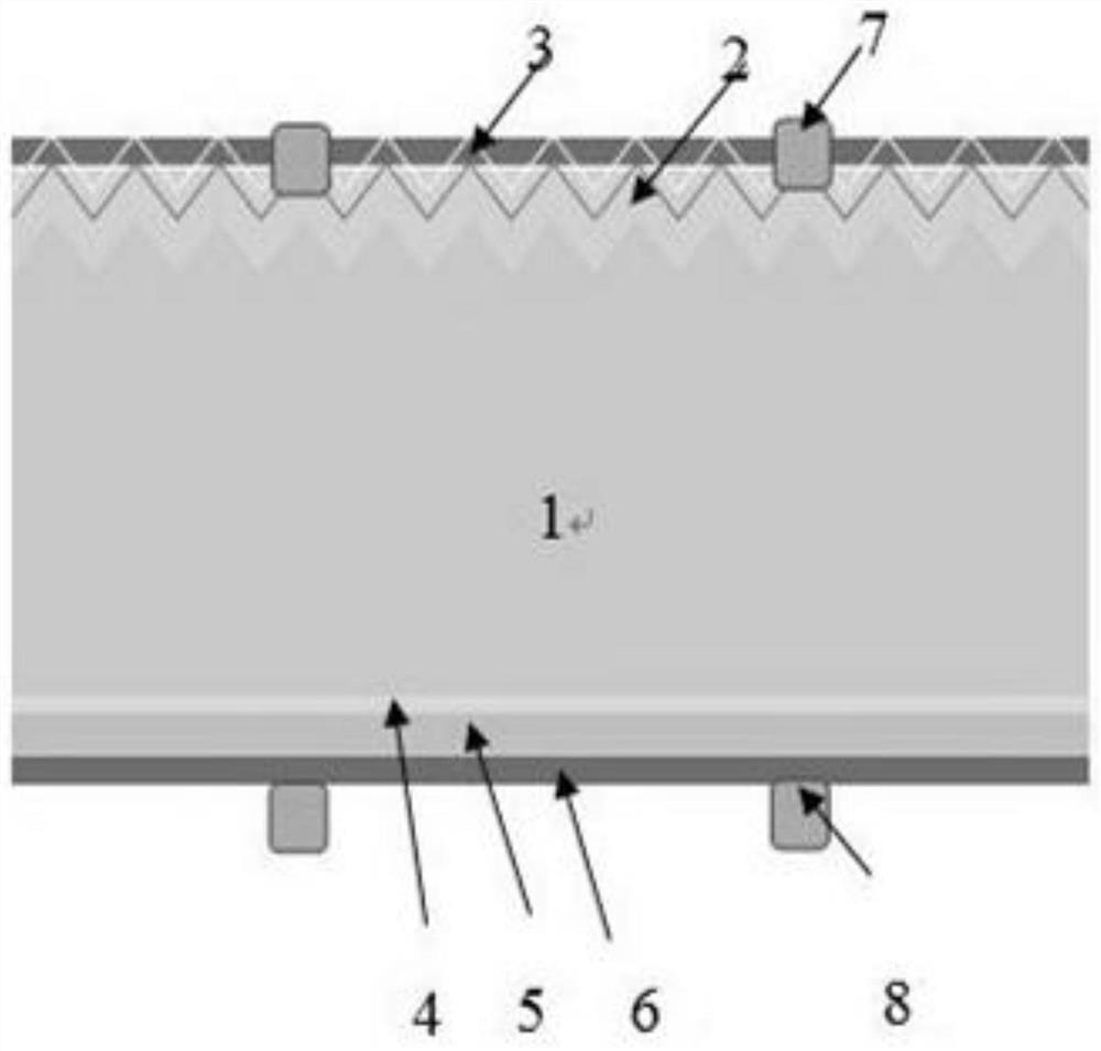
[0046] see figure 1 , the low-cost high-efficiency solar cell in the present invention includes a substrate 1, and the substrate 1 is an N-type substrate,
[0047] The diffusion layer 2 located on the upper surface of the substrate, the diffusion layer 2 is an n+ layer,
[0048] The passivation layer 3 located on the upper surface of the diffusion layer, the passivation layer 3 is a stack of silicon oxide / silicon nitride,
[0049] a silicon oxide layer 4 located on the lower surface of the substrate,
[0050] The doped polysilicon layer 5 located on the lower surface of the silicon oxide layer is a p+ polysilicon layer.
[0051] The hydrogenated transparent conductive film 6 located on the lower surface of the doped polysilicon layer, the hydrogenated transparent conductive film 6 is selected from AZO:H.
[0052] As well as the upper electrode 7 located on the upper surface of the passivation layer and the lower electrode 8 located on the lower surface of the hydrogenated t...
Embodiment 2
[0064] see figure 1 , the low-cost high-efficiency solar cell in the present invention includes a substrate 1, and the substrate 1 is an N-type substrate,
[0065] The diffusion layer 2 located on the upper surface of the substrate, the diffusion layer 2 is a p+ layer,
[0066] The passivation layer 3 located on the upper surface of the diffusion layer, the passivation layer 3 is a stack of silicon oxide / aluminum oxide / silicon nitride,
[0067] a silicon oxide layer 4 located on the lower surface of the substrate,
[0068] The doped polysilicon layer 5 located on the lower surface of the silicon oxide layer, the doped polysilicon layer 5 is an n+ polysilicon layer,
[0069] The hydrogenated transparent conductive film 6 located on the lower surface of the doped polysilicon layer, the hydrogenated transparent conductive film 6 is selected from AZO:H.
[0070] And the upper electrode 7 located on the upper surface of the passivation layer and the lower electrode 8 located on ...
Embodiment 3
[0082] see figure 1 , the low-cost high-efficiency solar cell in the present invention includes a substrate 1, and the substrate 1 is an N-type substrate,
[0083] The diffusion layer 2 located on the upper surface of the substrate, the diffusion layer 2 is a p+ layer,
[0084] The passivation layer 3 located on the upper surface of the diffusion layer, the passivation layer 3 is a stack of silicon oxide / aluminum oxide / silicon nitride,
[0085] a silicon oxide layer 4 located on the lower surface of the substrate,
[0086] The doped polysilicon layer 5 located on the lower surface of the silicon oxide layer, the doped polysilicon layer 5 is an n+ polysilicon layer,
[0087] The hydrogenated transparent conductive film 6 located on the lower surface of the doped polysilicon layer, the hydrogenated transparent conductive film 6 is 10:H.
[0088] And the upper electrode 7 located on the upper surface of the passivation layer and the lower electrode 8 located on the lower surfa...
PUM
| Property | Measurement | Unit |
|---|---|---|
| thickness | aaaaa | aaaaa |
| thickness | aaaaa | aaaaa |
| thickness | aaaaa | aaaaa |
Abstract
Description
Claims
Application Information
 - Generate Ideas
- Intellectual Property
- Life Sciences
- Materials
- Tech Scout
- Unparalleled Data Quality
- Higher Quality Content
- 60% Fewer Hallucinations
Browse by: Latest US Patents, China's latest patents, Technical Efficacy Thesaurus, Application Domain, Technology Topic, Popular Technical Reports.
© 2025 PatSnap. All rights reserved.Legal|Privacy policy|Modern Slavery Act Transparency Statement|Sitemap|About US| Contact US: help@patsnap.com


