
Silicon-based MEMS optical switch based on electrostatic comb driving, and N * N array

An optical switch array, optical switch technology, applied in the direction of light guide, optics, optical components, etc., can solve the problem of long switching time and so on

Active Publication Date: 2021-02-02
ZHEJIANG UNIV
View PDF7 Cites 1 Cited by
  • Summary
  • Abstract
  • Description
  • Claims
  • Application Information

AI Technical Summary

Problems solved by technology

Traditional 3D MEMS-based switches have good scalability (hundreds of input / output ports), low insertion loss and low crosstalk, but long switching time (several milliseconds or tens of milliseconds)

Method used


Image

  • Silicon-based MEMS optical switch based on electrostatic comb driving, and N * N array
  • Silicon-based MEMS optical switch based on electrostatic comb driving, and N * N array
  • Silicon-based MEMS optical switch based on electrostatic comb driving, and N * N array

Examples


Embodiment 1

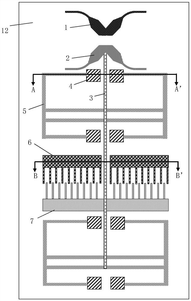
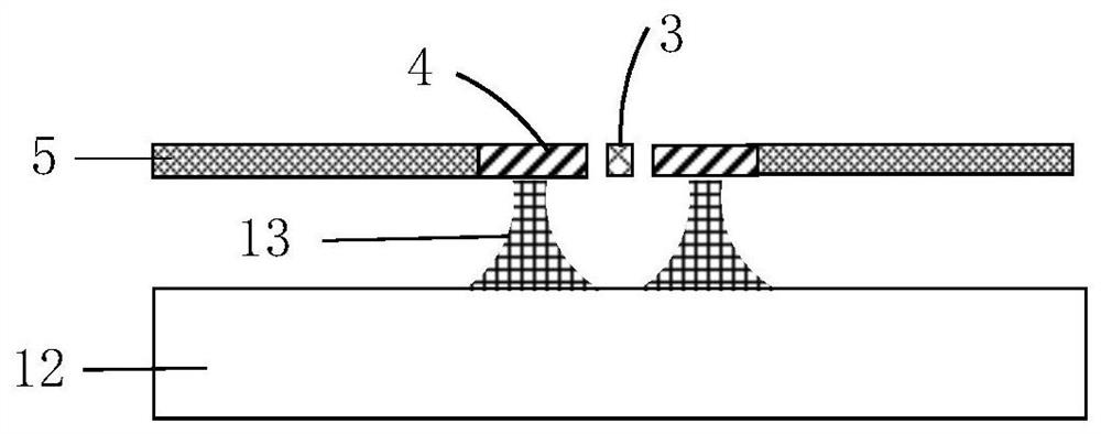
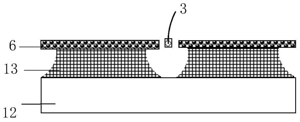
[0050] Such as figure 1 and Figure 4 As shown, the electrostatic comb driver of this embodiment is mainly composed of a pair of electrostatic comb teeth 6, 7, a first island spring structure, a second island spring structure and a transmission rod 3; The direction of movement is arranged. One end of the transmission rod 3 is fixedly connected to the movable cross waveguide mirror 2, specifically connected to the V-shaped intersection of the wide waveguide of the movable cross waveguide mirror 2. The transmission rod 3 is perpendicular to the total reflection surface of the movable cross waveguide mirror 2. A first island spring structure, a pair of electrostatic comb teeth 6, 7 and a second island spring structure are sequentially provided from the movable cross waveguide mirror 2 to the other end of the transmission rod 3 .

[0051] The structure of the first island spring structure and the second island spring structure are the same, both including four fixed islands 4 and...

Embodiment 2

[0062] Such as Figure 5 and Figure 6 As shown, the electrostatic comb driver of this embodiment is a bistable electrostatic comb driver, which is mainly composed of an electrostatic comb group, a third island spring structure, a fourth island spring structure and a transmission rod 3; the transmission rod 3 moves along the cross The moving direction of the waveguide mirror 2 is arranged. One end of the transmission rod 3 is fixedly connected to the movable cross waveguide mirror 2, specifically connected to the V-shaped intersection of the wide waveguide of the movable cross waveguide mirror 2. The transmission rod 3 and the movable cross waveguide mirror 2 The total reflection surface is vertical, and the third island spring structure, the electrostatic comb group and the fourth island spring structure are arranged sequentially from the movable cross waveguide mirror 2 to the other end of the transmission rod 3; the third island spring structure and the fourth island spring...


PUM

PropertyMeasurementUnit
Thicknessaaaaaaaaaa
Thicknessaaaaaaaaaa
Extinction ratioaaaaaaaaaa

Abstract

The invention discloses a silicon-based waveguide MEMS optical switch based on electrostatic comb driving, and an N * N array. The optical switch is mainly composed of two separated crossed waveguidemirrors and an electrostatic comb drive. A crossed waveguide is composed of two crossed wide waveguides and four heat insulation conical waveguides; the electrostatic comb drive comprises an electrostatic comb, an island spring structure and a transmission rod; the electrostatic comb is of a pair of comb tooth structures, and other parts of the electrostatic comb are kept grounded by applying voltage to fixed comb teeth; and under the action of electrostatic force, the movable comb teeth move towards the fixed comb teeth, a spring deforms, the movable crossed waveguide mirror is pushed by thetransmission rod to move towards the fixed crossed waveguide mirror, and the separated crossed waveguide mirror is recombined into a complete crossed waveguide. The output optical path of the opticalswitch is regulated and controlled by the electrostatic comb drive, the 2 * 2 optical switch unit with low loss and high extinction ratio and the N * N array are finally realized, and the optical switch has the outstanding advantages of large bandwidth, low loss, high extinction ratio, low energy consumption, simple structure, convenience in control, simple and convenient process and the like.

Description

technical field [0001] The invention belongs to the field of integrated optoelectronic devices, and specifically relates to a silicon-based waveguide MEMS optical switch and array, in particular to an integrated silicon-based waveguide MEMS capable of controlling the movement of crossed waveguide mirrors through electrostatic comb driving to regulate the transmission direction of light Optical switches and arrays. Background technique [0002] With the accelerated and mature application of next-generation information technologies such as 5G, Internet of Things, big data, and artificial intelligence, the scale of data center networks continues to expand, and warehouse-level large-scale data centers containing tens of thousands or even hundreds of thousands of servers are developing rapidly. With the rapid increase in traffic, it is urgent to develop a new generation of big data centers to provide strong support for the development of the digital economy. In response to this ...

Claims


Application Information

Patent Timeline
IPC IPC(8): G02B6/35G02B26/08
CPCG02B6/3518G02B6/3546G02B6/3586G02B26/0841
Inventor 戴道锌孙仪李欢
Owner ZHEJIANG UNIV
Learn More