
Element embedded packaging method and integrated circuit component

A packaging method and embedded technology, applied in the direction of assembling printed circuits with electrical components, printed circuits connected with non-printed electrical components, electrical components, etc., can solve problems such as insufficient filling, increase filling volume, and be operable Strong, improve the effect of filling uniformity

Pending Publication Date: 2021-01-29
安捷利美维电子(厦门)有限责任公司 +1
View PDF0 Cites 0 Cited by
  • Summary
  • Abstract
  • Description
  • Claims
  • Application Information

AI Technical Summary

Problems solved by technology

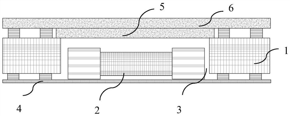
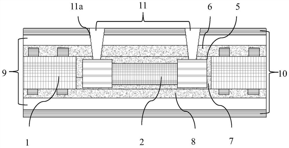
[0004] The technical problem to be solved by the present invention is to provide a component embedded packaging method and integrated circuit components to solve the problem of insufficient filling when embedding components in the PCB board, especially the filling when embedding thicker components in the PCB question

Method used


Image

  • Element embedded packaging method and integrated circuit component
  • Element embedded packaging method and integrated circuit component
  • Element embedded packaging method and integrated circuit component

Examples


Embodiment Construction

[0039] The specific implementation manners of the present invention will be further described in detail below in conjunction with the accompanying drawings and embodiments. The following examples are used to illustrate the present invention, but are not intended to limit the scope of the present invention.

[0040] Unless otherwise defined, all technical and scientific terms used herein have the same meaning as commonly understood by one of ordinary skill in the technical field of the invention. The terminology used herein in the description of the present invention is only for the purpose of describing specific embodiments, and is not intended to restrict the present invention.

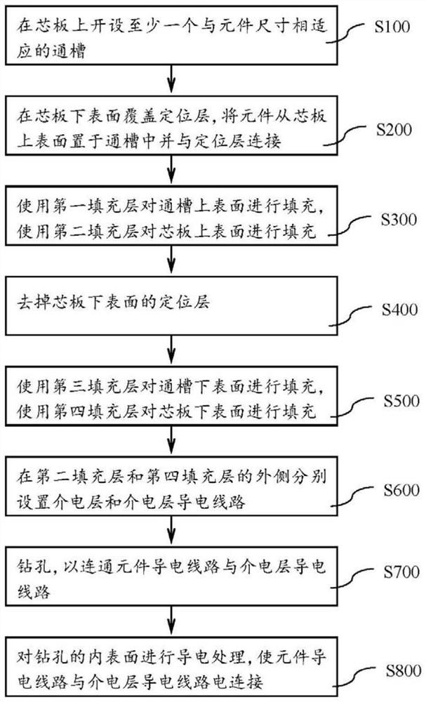
[0041] Such as figure 1 As shown, a component embedded packaging method and an integrated circuit component according to a preferred embodiment of the present invention, wherein the method includes the following steps:

[0042] S100. Opening through slots on the core board, the size of the opening ...


PUM


Abstract

The invention relates to the technical field of PCB packaging, and discloses an element embedded packaging method and an integrated circuit component, and the method comprises the following steps: forming a through groove in a core plate; covering the lower surface of the core plate with a positioning layer to position a element; filling the upper surface of the through groove with a first fillinglayer, and filling the upper surface of the core plate with a second filling layer; removing the positioning layer on the lower surface of the core plate; filling the lower surface of the through groove with a third filling layer, and filling the lower surface of the core plate with a fourth filling layer; arranging a dielectric layer and a dielectric layer conducting circuit on the outer sides of the second filling layer and the fourth filling layer respectively; drilling; and performing conducting treatment on the inner surface of the drilled hole. The element embedded packaging method andthe integrated circuit component have the advantages that a local reinforcing and filling method is added in the pressing process of a PCB, a gap with a large depth ratio between an element and a groove cavity is supplemented and filled in a targeted manner in a local range, and a reinforcing adhesive layer with a small area increases the filling amount and improves the filling uniformity.

Description

technical field [0001] The invention relates to the technical field of PCB board packaging, in particular to an element embedding method of a printed circuit board and an integrated circuit component. Background technique [0002] With the development trend of electronic products to small size and high performance, PCB printed circuit boards need to carry more and more electronic components, and the surface space of PCB printed boards is limited, so more and more components originally mounted on PCB printed circuit boards The electronic components on the surface of the board are directly packaged into the PCB board by embedding, which can save surface mounting space, reduce product volume, and improve performance. [0003] The prior art has provided relatively mature methods for embedding components in the core board of the PCB. However, due to thinner and lighter electronic products, the method provided by the prior art is also an embedding method for relatively thinner an...

Claims


Application Information

Patent Timeline
Patent Type & Authority Applications(China)
IPC IPC(8): H05K1/18H05K3/32
CPCH05K1/185H05K1/188H05K3/32H05K2203/1316
Inventor 陈俭云白杨吴少晖岑文锋邓朝松何亚志孔令文
Owner 安捷利美维电子(厦门)有限责任公司
Learn More