Detection device based on energy conservation of chip on financial electronic circuit board

A technology for electronic circuit boards and detection devices, which is applied in the direction of electronic circuit testing, measuring devices, measuring electricity, etc., can solve problems such as waste of manpower, missed detection, wrong detection, small pins of chips, etc., so as to facilitate removal and processing, prevent The effect of missed detection and accurate detection effect

Inactive Publication Date: 2020-12-29
南京禄廖社电子商务有限公司
View PDF0 Cites 0 Cited by
  • Summary
  • Abstract
  • Description
  • Claims
  • Application Information

AI Technical Summary

Problems solved by technology

[0002] E-finance is a financial activity that exists in the electronic space. Its existence is virtualized and its operation mode is networked. In the chip manufacturing process, there is a process of wafer packaging, which is to weld the wafer to the metal After the welding is completed, a layer of glue is added to the surface of the wafer to protect the wafer. The chip is installed on the corresponding groove of the card body. When the position and height of the chip are consistent with the position and depth of the groove When there is a mismatch, a part of the wafer will be exposed, which will make the chip invalid. Therefore, the chip cannot be directly loaded into the product. If there is a problem with the overall debugging of the product, it needs to be disassembled and repaired, resulting in a waste of manpower. Generally speaking, the processing factory will conduct all or sampling inspections on the chips on the circuit boards of electronic products before assembling the products.
[0003] However, since the pins of the chip are generally small, it is difficult to detect such problems manually. If it is directly installed in the product, it needs to be disassembled and replaced if there is a problem, which will affect the production efficiency. The detection of the chip is generally done manually. It is relatively boring and cumbersome, and it is a simple repetitive labor. In actual operation, problems such as missed detection and wrong detection are prone to occur. Therefore, those skilled in the art provide a detection device based on energy-saving chips on financial electronic circuit boards to solve the above background. questions raised in technology

Method used


Image

  • Detection device based on energy conservation of chip on financial electronic circuit board
  • Detection device based on energy conservation of chip on financial electronic circuit board
  • Detection device based on energy conservation of chip on financial electronic circuit board

Examples


Embodiment Construction

[0021] The following will clearly and completely describe the technical solutions in the embodiments of the present invention with reference to the accompanying drawings in the embodiments of the present invention. Obviously, the described embodiments are only some, not all, embodiments of the present invention. Based on the embodiments of the present invention, all other embodiments obtained by persons of ordinary skill in the art without making creative efforts belong to the protection scope of the present invention.

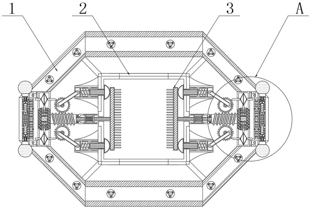
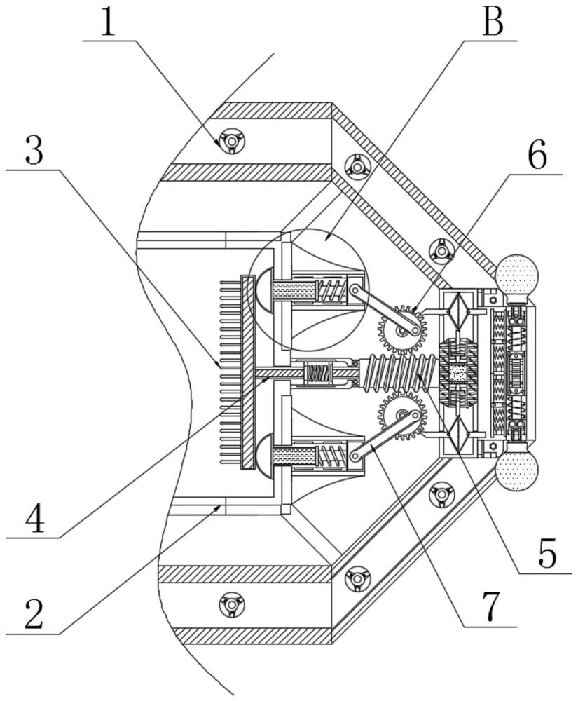
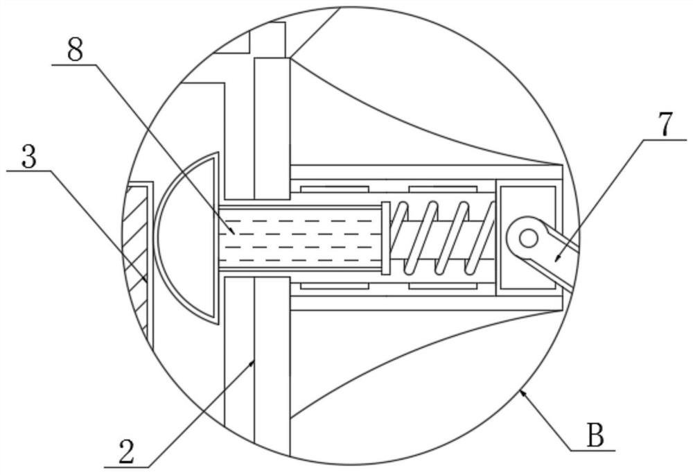
[0022] see Figure 1-6 , a detection device based on chip energy-saving on a financial electronic circuit board, comprising a fixed frame 1, the upper surface of the fixed frame 1 is fixedly connected with a detection frame 2, the outer wall of the detection frame 2 is movably connected with a first guide plate 4, and the first guide plate One end of 4 is fixedly connected with a detection plate 3 at the inner side of the detection frame 2, the other end of th...


PUM


Abstract

The invention relates to the technical field of electronic detection, in particular to a detection device based on energy conservation of a chip on a financial electronic circuit board. The outer wallof a detection frame is movably connected with a first guide plate in a penetrating mode, a detection plate is fixedly connected to one end of the first guide plate and located on the inner side of the detection frame, the other end of the first guide plate is fixedly and movably connected with a threaded rod, the upper side and the lower side of the threaded rod are meshed with gears, the upperends and the lower ends of the gears are meshed with connecting rods, and one ends of the connecting rods are movably connected with touch plates. When pins of the chip are not well installed and welded and a wafer is exposed, a circuit connected with the detection plate forms a closed loop, then a baffle is driven to be close to and clamped between racks of the gears, the gears stop rotating, atthe moment, the chip can be clamped in the detection plate all the time and cannot be moved away along with an assembly line, a worker can conveniently take out the chip for processing, the accurate detection effect is achieved, and the situations of missing detection and wrong detection are prevented.

Description

technical field [0001] The invention relates to the technical field of electronic detection, in particular to a detection device based on chip energy saving on a financial electronic circuit board. Background technique [0002] E-finance is a financial activity that exists in the electronic space. Its existence form is virtualized and its operation mode is networked. In the chip manufacturing process, there is a process of wafer packaging, which is to weld the wafer to the metal After the welding is completed, a layer of glue is added to the surface of the wafer to protect the wafer. The chip is installed on the corresponding groove of the card body. When the position and height of the chip are consistent with the position and depth of the groove When there is a mismatch, a part of the wafer will be exposed, which will invalidate the chip. Therefore, the chip cannot be directly loaded into the product. If there is a problem with the overall debugging of the product, it needs...

Claims


Application Information

Patent Timeline
Patent Type & Authority Applications(China)
IPC IPC(8): G01R31/28G01R31/01
CPCG01R31/01G01R31/2893G01R31/2896
Inventor 王颖
Owner 南京禄廖社电子商务有限公司
Why Eureka
Try Eureka