Manufacturing method of three-dimensional memory
A manufacturing method and memory technology, applied in the direction of electrical components, etc., can solve the problems of not being able to provide bit density, competition, etc.
- Summary
- Abstract
- Description
- Claims
- Application Information
AI Technical Summary
Problems solved by technology
Method used
Image
Examples
Embodiment Construction
[0085] In order to make the technical solutions and advantages of the embodiments of the present invention more clear, the specific technical solutions of the invention will be further described in detail below in conjunction with the drawings in the embodiments of the present invention.
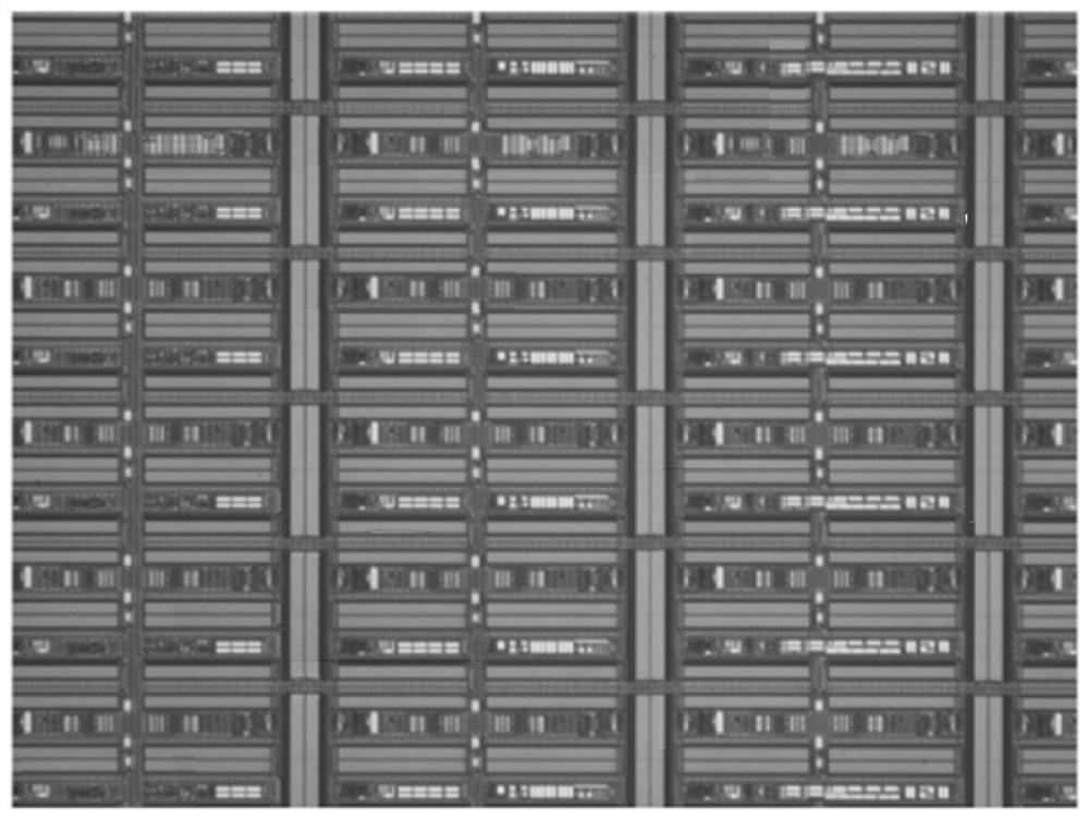
[0086] figure 1 It is a schematic diagram of a three-dimensional phase-change memory cell array observed by a scanning electron microscope. From figure 1 It can be seen that the three-dimensional phase change memory chip is composed of a plurality of small memory cell array blocks with a single bit line, word line and memory cells. A three-dimensional phase-change memory generally includes a top bit line, a word line, a bottom bit line, and a memory cell located at the intersection of the bit line and the word line. In practical applications, the word line, top bit line and bottom bit line are usually formed by a 20nm / 20nm line width (L / S, line / space) formed after the patterning process. ...
PUM
 Abstract
Description
Claims
Application Information
 - R&D
- Intellectual Property
- Life Sciences
- Materials
- Tech Scout
- Unparalleled Data Quality
- Higher Quality Content
- 60% Fewer Hallucinations
Browse by: Latest US Patents, China's latest patents, Technical Efficacy Thesaurus, Application Domain, Technology Topic, Popular Technical Reports.
© 2025 PatSnap. All rights reserved.Legal|Privacy policy|Modern Slavery Act Transparency Statement|Sitemap|About US| Contact US: help@patsnap.com


