Display device
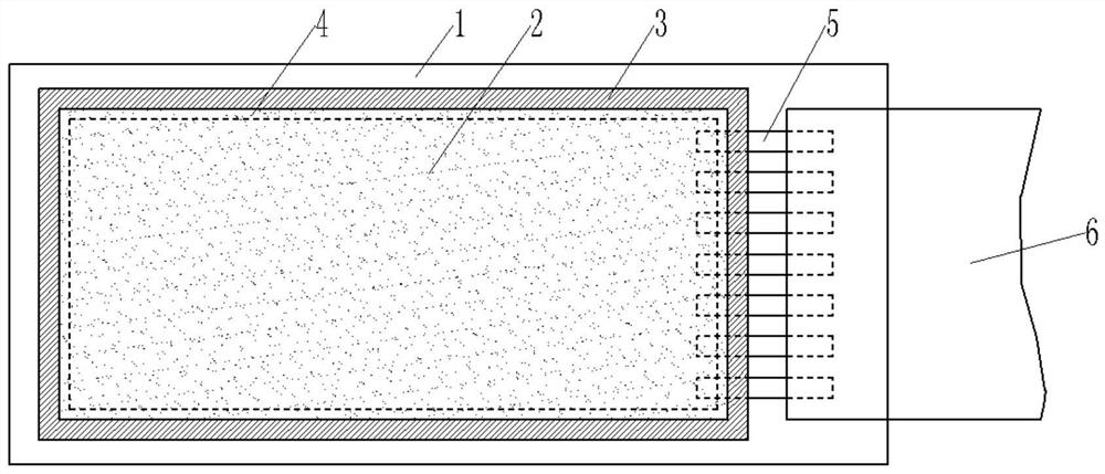
A technology for a display device and a display area, which is applied to semiconductor/solid-state device parts, semiconductor devices, electrical components, etc., can solve problems such as poor contact and chip-on-chip film 6 peeling, and achieve simplified structure, material saving, and simple structure Effect
- Summary
- Abstract
- Description
- Claims
- Application Information
AI Technical Summary
Problems solved by technology
Method used
Image
Examples
no. 1 example
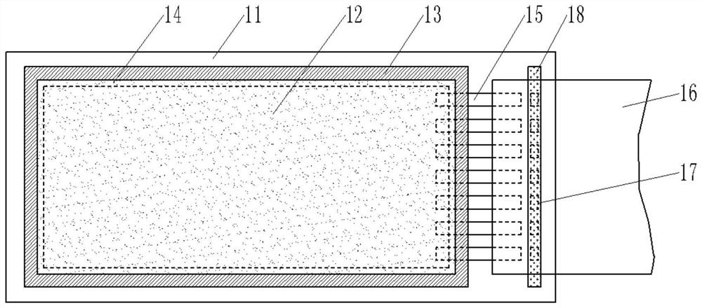
[0036] refer to image 3 and Figure 4 , the display device of this embodiment is different from the display device of the prior art in that it additionally has a pressing wall 18 . The setting of the pressure wall 18 is to ensure that the COF 16 will not be disconnected from the driving electrodes 15, so as to ensure reliable transmission of driving signals.
[0037] The display device includes a substrate 11, which may be formed of any suitable insulating material having flexibility. For example, it can be made of polyimide (PI), polycarbonate (PC), polyethersulfone (PES), polyethylene terephthalate (PET), polyethylene naphthalate (PEN) , polyarylate (PAR) or glass fiber reinforced plastic (FRP) and other polymer materials. The substrate 11 may also be rigid, such as glass.
[0038] The substrate 11 includes a display area and a non-display area, wherein the display area includes a display device 12, which may be an OLED display device, a mini-LED display device, and the...
no. 2 example
[0046] In this embodiment, no pressing wall is provided, and the improvement mainly lies in pressing the chip-on-chip film 16 by using the side walls of the cofferdam. see Figure 5 and Figure 6 , the bank dam 13 not only surrounds the display area, but also additionally surrounds the non-display area, which has a side wall in the non-display area, a part of which is bonded to the substrate 11 through a plurality of openings 17 in the chip-on-chip film 16 , so as to ensure the bonding force of the joint and reduce the risk of peeling.
[0047]In this embodiment, the side wall includes a first portion with a wider cross-section and a second portion with a narrower cross-section. The narrower second portion is located in the plurality of openings 17 , and the first portion is located on the COF 16 . Moreover, the plurality of openings 17 are arranged on the extension lines of the plurality of driving electrodes 15 in one-to-one correspondence, so as to further strengthen the...
no. 3 example
[0050] In the first embodiment, the pressing wall 18 is only bonded to the substrate 11 at the openings 17 , the bonding force is relatively small, and there is no protection for the driving electrodes 15 . In this embodiment, the shape of the pressing wall 19 is an inverted T shape, and its wider first part is attached to the substrate 11, and its narrower second part passes through the plurality of openings 17, wherein Both the first part and the second part are integrally formed by injection molding.
PUM
 Abstract
Description
Claims
Application Information
 - R&D
- Intellectual Property
- Life Sciences
- Materials
- Tech Scout
- Unparalleled Data Quality
- Higher Quality Content
- 60% Fewer Hallucinations
Browse by: Latest US Patents, China's latest patents, Technical Efficacy Thesaurus, Application Domain, Technology Topic, Popular Technical Reports.
© 2025 PatSnap. All rights reserved.Legal|Privacy policy|Modern Slavery Act Transparency Statement|Sitemap|About US| Contact US: help@patsnap.com


