
LED chip test fixture, test method and test system

A technology of LED chips and test fixtures, which is applied in the direction of electronic circuit testing, measuring electronics, measuring devices, etc., can solve the problems that the accuracy rate is difficult to meet the demand, and achieve high accuracy rate, simple and fast test process, and high test efficiency.

Active Publication Date: 2020-11-13
深圳市TCL高新技术开发有限公司
View PDF9 Cites 9 Cited by
  • Summary
  • Abstract
  • Description
  • Claims
  • Application Information

AI Technical Summary

Problems solved by technology

[0006] The purpose of the present invention is to provide a LED chip test fixture, test method and test system to solve the problem that the accuracy of traditional test methods is difficult to meet the demand

Method used


Image

  • LED chip test fixture, test method and test system
  • LED chip test fixture, test method and test system
  • LED chip test fixture, test method and test system

Examples


Embodiment Construction

[0052] In order to make the technical problems, technical solutions and beneficial effects to be solved by the present invention clearer, the present invention will be further described in detail below in conjunction with the accompanying drawings and embodiments. It should be understood that the specific embodiments described here are only used to explain the present invention, not to limit the present invention.

[0053] It should be noted that when an element is referred to as being “fixed” or “disposed on” another element, it may be directly on the other element or be indirectly on the other element. When an element is referred to as being "connected to" another element, it can be directly connected to the other element or indirectly connected to the other element.

[0054] It is to be understood that the terms "length", "width", "top", "bottom", "front", "rear", "left", "right", "vertical", "horizontal", "top" , "bottom", "inner", "outer" and other indicated orientations...


PUM


Abstract

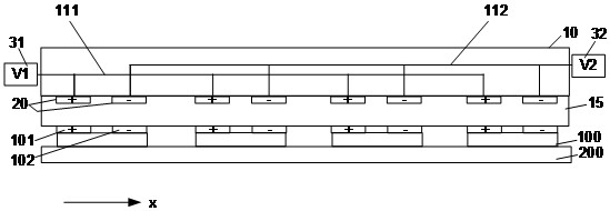
The invention relates to an LED chip test fixture, a test method and a test system. The LED chip test fixture provides a substrate on which a test electrode is laid, an electrolyte layer on the substrate is attached to a chip film on which LED chips arranged in an array manner are laid, therefore, a positive test electrode and a negative test electrode are respectively aligned with the corresponding electrodes of the LED chip to be tested. The LED chip test fixture is advantaged in that an LED chip testing jig can be used for testing the photoelectric characteristics of a large number of LED chips, and the LED chip testing jig is convenient, simple and high in accuracy.

Description

technical field [0001] The invention belongs to the technical field of light emitting diode (English: Light Emitting Diode, LED for short) testing, and more specifically relates to an LED chip testing fixture, testing method and testing system. Background technique [0002] Miniaturized (English: Micro) LED chips can be used in direct view (English: Direct View) display technology to form a light-emitting unit, which has the advantages of high brightness, wide color gamut, high stability, long life, energy saving, and transparency. However, there are still many technical difficulties that need to be resolved before the mass production of miniaturized LED display technology, and the photoelectric characteristic test is one of the difficulties. [0003] On the one hand, the repair cost of miniaturized Micro LED chips used in direct-view display technology is very high, so it must have a high yield rate when placed on the target backplane in order to reduce the number of repair...

Claims


Application Information

Patent Timeline
Patent Type & Authority Applications(China)
IPC IPC(8): G01R31/28
CPCG01R31/2891G01R31/2898G01R31/2887
Inventor 林智远闫晓林
Owner 深圳市TCL高新技术开发有限公司
Learn More