Vertical structure LED chip with novel electrode wire arrangement
A LED chip and vertical structure technology, applied in the direction of circuits, electrical components, electric solid devices, etc., can solve the problems of LED light efficiency, heat dissipation and stability limitations, to increase the effective light output area, increase the light emitting area, and large heat dissipation area effect
- Summary
- Abstract
- Description
- Claims
- Application Information
AI Technical Summary
Problems solved by technology
Method used
Image
Examples
Embodiment 1
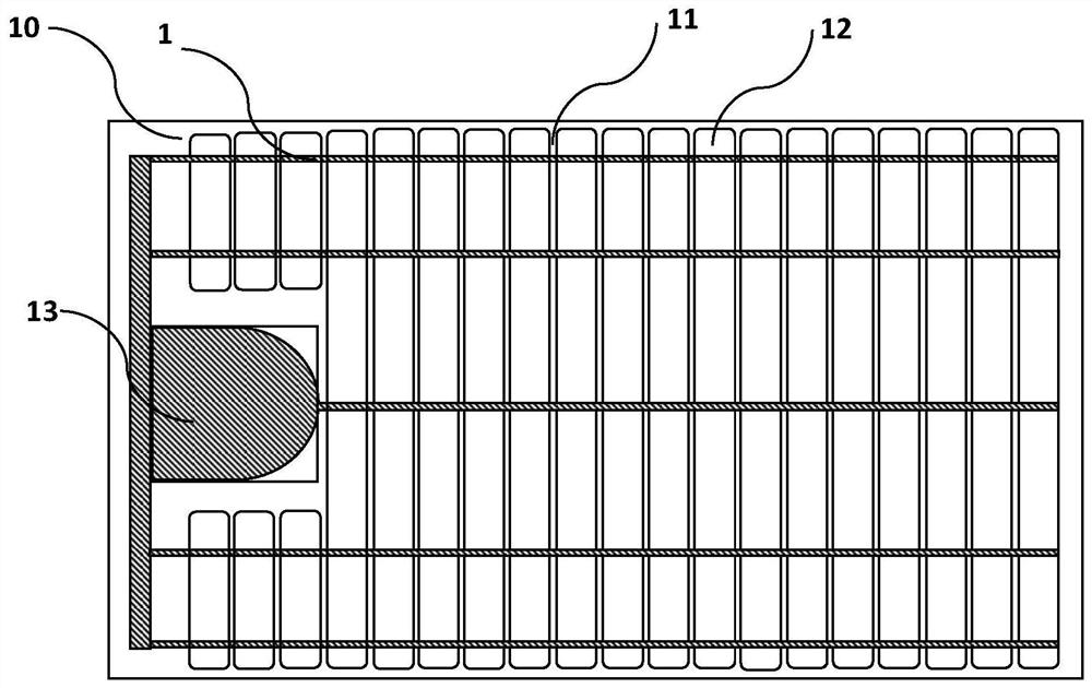
[0049] This embodiment provides a novel vertical structure LED chip with electrode wire arrangement, including: second conductivity type electrode wire 1, diode mesa structure 10, diode unit 12, trench structure 11 and second conductivity type pad 13. The trench structure 11 is located between the diode units and has a rectangular shape. The electrode lines of the second conductivity type extend from the front face to the rear face of each diode unit; the area of the mesa structure is determined according to the current diffusion length. The pad of the second conductivity type has a thickness of 0.001 micron to 20 micron, and a width of 10 micron to 100 micron. The pads of the second conductivity type are connected to the electrode lines of the second conductivity type; the electrode lines of the second conductivity type are line-shaped connection lines. The second conductive type electrode line has a width of 0.001-20 microns and a thickness of 0.001-10 microns. The electr...
Embodiment 2
[0056] This embodiment provides a novel vertical structure LED chip with electrode wire arrangement, including: second conductivity type electrode wire 1, diode mesa structure 10, diode unit 12, trench structure 11 and second conductivity type pad 13. The trench structure 11 is located between the diode units, and the electrode lines of the second conductivity type extend from the front end to the rear end of each diode unit, or extend from the front end to the rear end of some diode units; the area of the mesa structure is determined according to the current diffusion length . The pad of the second conductivity type has a thickness of 0.001 micron to 20 micron, and a width of 10 micron to 100 micron. The pads of the second conductivity type are connected to the electrode lines of the second conductivity type; the electrode lines of the second conductivity type are line-shaped connection lines. The width of the electrode lines of the second conductivity type is 0.001-20 mic...
PUM
| Property | Measurement | Unit |
|---|---|---|
| length | aaaaa | aaaaa |
| thickness | aaaaa | aaaaa |
| width | aaaaa | aaaaa |
Abstract
Description
Claims
Application Information
 - Generate Ideas
- Intellectual Property
- Life Sciences
- Materials
- Tech Scout
- Unparalleled Data Quality
- Higher Quality Content
- 60% Fewer Hallucinations
Browse by: Latest US Patents, China's latest patents, Technical Efficacy Thesaurus, Application Domain, Technology Topic, Popular Technical Reports.
© 2025 PatSnap. All rights reserved.Legal|Privacy policy|Modern Slavery Act Transparency Statement|Sitemap|About US| Contact US: help@patsnap.com


