Method for preparing organic photovoltaic device with super-thick absorption layer and organic photovoltaic device
A technology of organic photovoltaic devices and absorbing layers, which is applied in photovoltaic power generation, electric solid-state devices, semiconductor devices, etc., can solve the problem of low overall performance, achieve device performance optimization, simple and easy-to-operate preparation process, and low manufacturing cost.
- Summary
- Abstract
- Description
- Claims
- Application Information
AI Technical Summary
Problems solved by technology
Method used
Image

Examples
Embodiment 1
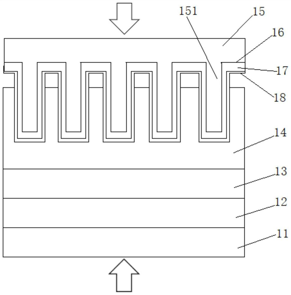
[0022] Such as figure 1 As shown, this embodiment provides a method for preparing an organic photovoltaic device with an ultra-thick absorbing layer, including step S1: preparing the device, respectively preparing the first device bottom and the first device top of the device, and the first device bottom includes: A first substrate 11, a first electrode 12 on the first substrate 11, a hole transport layer 13 on the first electrode 12, an ultra-thick absorption layer 14 on the hole transport layer 13; The top of the first device includes: a second substrate 15, an adhesive layer on the surface of the second substrate 15, a second electrode 17 on the adhesive layer 16, a second electrode 17 on the second electrode 17 The electron transport layer 18, the second substrate 15 is provided with a plurality of protrusions 151 along the length direction; step S2: pressing the top of the first device on the bottom of the first device, so that the protrusions 151 extend into the ultra-t...
Embodiment 2
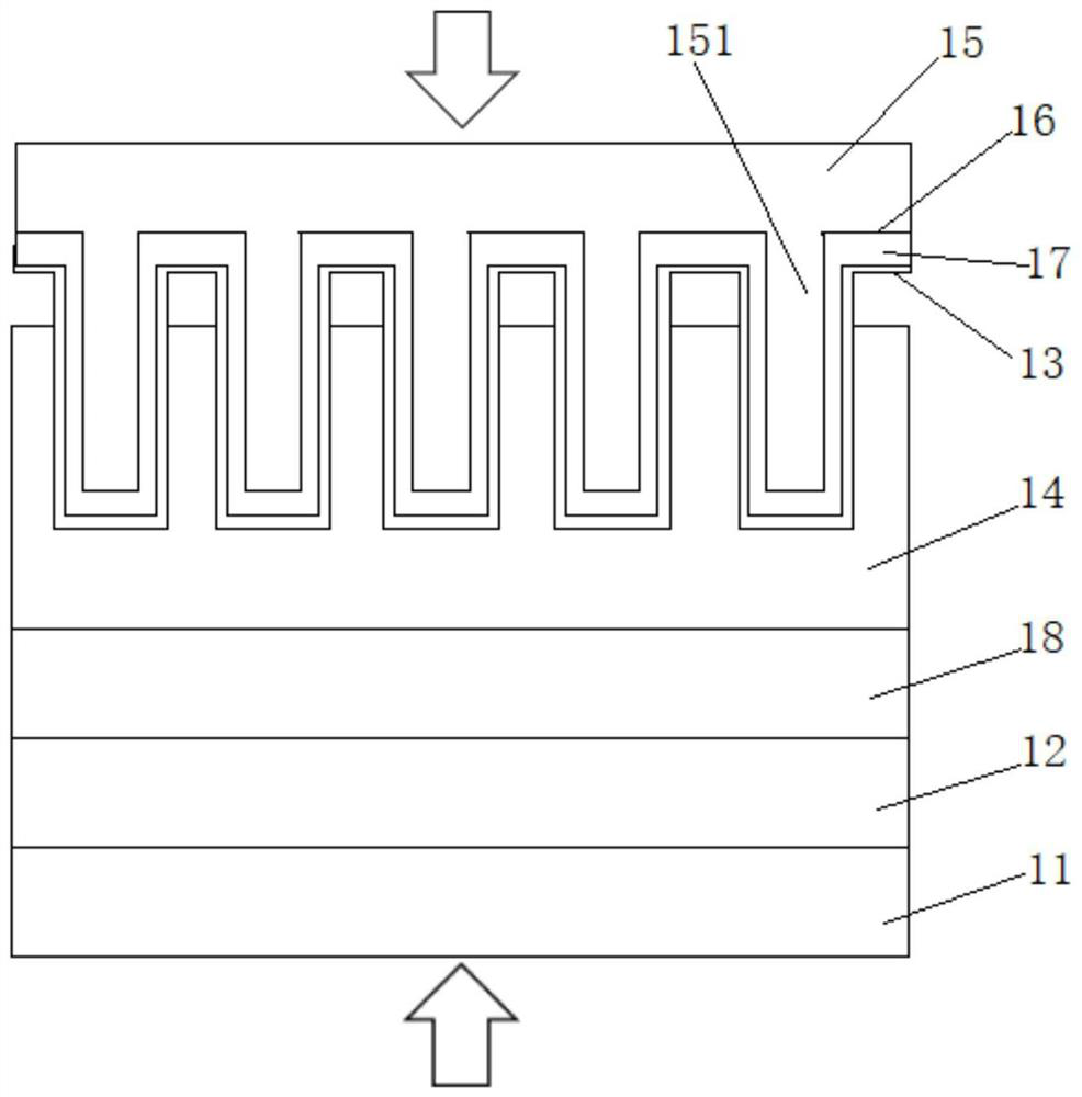
[0047] Such as figure 2 As shown, this embodiment provides a method for preparing an organic photovoltaic device with an ultra-thick absorbing layer, including the following steps: Step S1: preparing the device, respectively preparing the bottom of the second device and the top of the second device, and the second device The bottom includes: a first substrate 11, a first electrode 12 on the first substrate 11, an electron transport layer 18 on the first electrode 11, an ultra-thick absorption layer 14 on the electron transport layer 18 The top of the second device includes: a second substrate 15, an adhesive layer 16 on the surface of the second substrate 15, a second electrode 17 on the adhesive layer 16, and a second electrode 17 on the second electrode 17 The hole transport layer 13 on the second substrate 15 is provided with a plurality of protrusions 151 along the length direction; step S2: pressing the top of the second device on the bottom of the second device, so that...
Embodiment 3
[0057] Such as figure 1 As shown, this embodiment provides an organic photovoltaic device with an ultra-thick absorption layer prepared by a lamination method, which is prepared according to the method for preparing an organic photovoltaic device with an ultra-thick absorption layer described in Example 1, including: the bottom of the first device and the top of the first device, the bottom of the first device includes: a first substrate 11, a first electrode 12 on the first substrate 11, a hole transport layer 13 on the first electrode 12, a The ultra-thick absorption layer 14 on the hole transport layer 13; the top of the first device includes: a second substrate 15, an adhesive layer 16 on the surface of the second substrate 15, an adhesive layer on the adhesive layer 16 The second electrode 17, the electron transport layer 18 located on the second electrode 17, the second substrate 15 is provided with a plurality of protrusions 151 along the length direction; the top of th...
PUM
| Property | Measurement | Unit |
|---|---|---|
| thickness | aaaaa | aaaaa |
| thickness | aaaaa | aaaaa |
| thickness | aaaaa | aaaaa |
Abstract
Description
Claims
Application Information
 - Generate Ideas
- Intellectual Property
- Life Sciences
- Materials
- Tech Scout
- Unparalleled Data Quality
- Higher Quality Content
- 60% Fewer Hallucinations
Browse by: Latest US Patents, China's latest patents, Technical Efficacy Thesaurus, Application Domain, Technology Topic, Popular Technical Reports.
© 2025 PatSnap. All rights reserved.Legal|Privacy policy|Modern Slavery Act Transparency Statement|Sitemap|About US| Contact US: help@patsnap.com