Copper-containing laminated film etching liquid for liquid crystal panel and application thereof
A liquid crystal panel and etching solution technology, applied in optics, instruments, nonlinear optics, etc., can solve problems such as high cost, achieve cost reduction, avoid bumping, and achieve good etching morphology
- Summary
- Abstract
- Description
- Claims
- Application Information
AI Technical Summary
Problems solved by technology
Method used
Image
Examples
Embodiment 1-5 and comparative example 1-4
[0093] The compositions of the etching solutions of Examples and Comparative Examples are shown in Table 1.
[0094] Table 1
[0095]
[0096]
[0097] Use a PP-lined stirred tank with a condenser to produce the above-mentioned etching solution main agent and auxiliary agent (see Table 1), and it can be used after passing the filter (the number of particles with a particle size above 0.5 μm is less than 100). During the production process, maintain the etching solution system below 45°C.
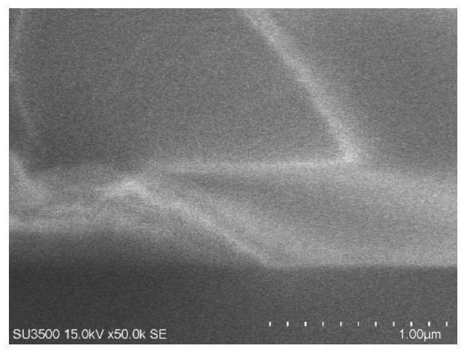
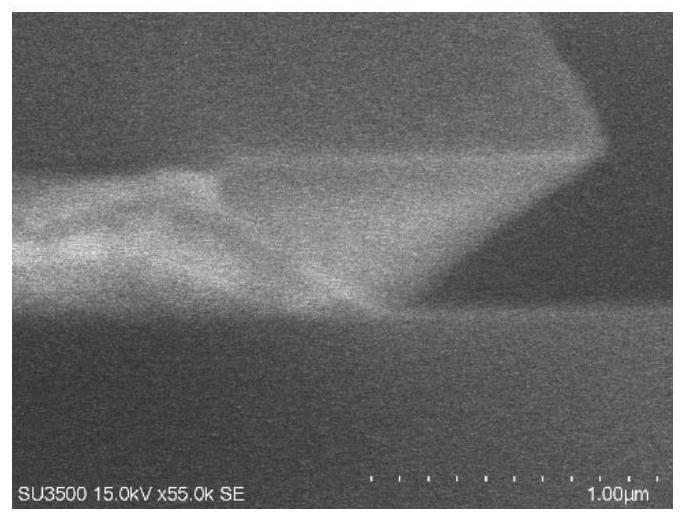
[0098] Use a hand-operated etching machine to etch a TFT substrate with a copper / molybdenum-niobium / IGZO film thickness of 4000 / 200 / 800A, and use different etching times to grasp the optimal etching time for the substrate.
PUM
 Abstract
Description
Claims
Application Information
 - R&D
- Intellectual Property
- Life Sciences
- Materials
- Tech Scout
- Unparalleled Data Quality
- Higher Quality Content
- 60% Fewer Hallucinations
Browse by: Latest US Patents, China's latest patents, Technical Efficacy Thesaurus, Application Domain, Technology Topic, Popular Technical Reports.
© 2025 PatSnap. All rights reserved.Legal|Privacy policy|Modern Slavery Act Transparency Statement|Sitemap|About US| Contact US: help@patsnap.com


