
A kind of semiconductor device and manufacturing method

A manufacturing method and semiconductor technology, applied in semiconductor devices, final product manufacturing, sustainable manufacturing/processing, etc., can solve problems such as difficulty in meeting high peak tunneling current, improve tunneling current, improve performance, and ensure material quality. Effect

Active Publication Date: 2021-11-23
SUZHOU EVERBRIGHT PHOTONICS CO LTD +1
View PDF6 Cites 0 Cited by
  • Summary
  • Abstract
  • Description
  • Claims
  • Application Information

AI Technical Summary

Problems solved by technology

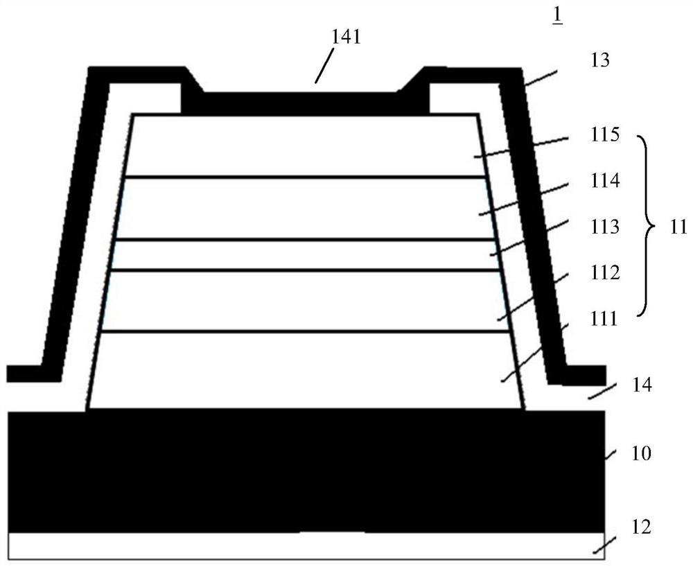
[0003] Therefore, the present invention provides a semiconductor device to solve the problem that the tunnel junction device in the prior art is difficult to meet the high tunneling peak current

Method used


Image

  • A kind of semiconductor device and manufacturing method
  • A kind of semiconductor device and manufacturing method

Examples


Embodiment Construction

[0034] The technical solutions of the present invention will be clearly and completely described below in conjunction with the accompanying drawings. Apparently, the described embodiments are some of the embodiments of the present invention, but not all of them. Based on the embodiments of the present invention, all other embodiments obtained by persons of ordinary skill in the art without making creative efforts belong to the protection scope of the present invention.

[0035] In the description of the present invention, it should be noted that the terms "center", "upper", "lower", "left", "right", "vertical", "horizontal", "inner", "outer" etc. The indicated orientation or positional relationship is based on the orientation or positional relationship shown in the drawings, and is only for the convenience of describing the present invention and simplifying the description, rather than indicating or implying that the referred device or element must have a specific orientation, ...


PUM

PropertyMeasurementUnit
thicknessaaaaaaaaaa
thicknessaaaaaaaaaa

Abstract

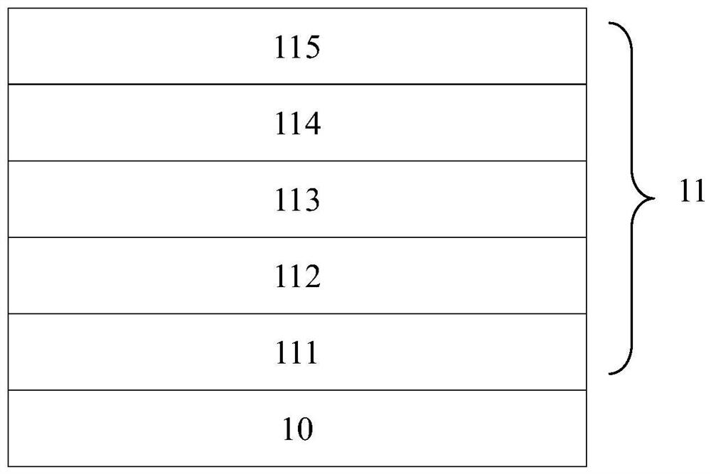
The invention discloses a semiconductor device and relates to the field of semiconductor optoelectronic devices. The semiconductor device disclosed in the present invention includes: a first conductivity type semiconductor layer; an insertion layer arranged on the first conductivity type semiconductor layer, the insertion layer is silicon-tellurium co-doped indium gallium arsenic; a second conductivity type is arranged on the insertion layer type semiconductor layer; wherein the first conductivity type and the second conductivity type are different conductivity types. The semiconductor device disclosed by the invention can realize higher tunneling peak current and can meet higher tunneling current requirement.

Description

technical field [0001] The invention relates to the field of semiconductor tunnel junctions, in particular to a semiconductor device containing silicon tellurium co-doped indium gallium arsenic insertion layer and a manufacturing method thereof. Background technique [0002] Tunnel junctions are key components of multijunction solar cells. In practical applications, the following conditions must be met: (1) The tunneling peak current of the tunnel junction must be higher than the device current; (2) The resistivity of the tunnel junction should be as low as possible; (3) It is transparent to the light passing through the optoelectronic device , cannot absorb light. The p-GaAs / n-GaAs tunnel junction is widely used in the connection of the solar spectrum absorption sub-junction through more than 867nm because of its easy material growth. In order to obtain high tunneling current and low resistivity, it is usually realized by heavy doping, but the doping concentration of Si-d...

Claims


Application Information

Patent Timeline
Patent Type & Authority Patents(China)
IPC IPC(8): H01L31/0352H01L31/0304H01L31/068H01L31/18
CPCH01L31/03042H01L31/035209H01L31/068H01L31/1844Y02E10/547Y02P70/50
Inventor 苟于单王俊程洋肖啸郭银涛
Owner SUZHOU EVERBRIGHT PHOTONICS CO LTD
Learn More