
Atomic-scale surface and structure ultra-short pulsed light efficient processing method

An ultra-short pulse, processing method technology, applied in metal processing equipment, manufacturing tools, laser welding equipment and other directions, can solve the problems of difficult to achieve atomic-level high precision, destroy the atomic arrangement of the extreme surface layer, hinder the manufacturing process, etc., to achieve flexible improvement. performance and efficiency, avoid lattice damage, and improve the effect of extreme precision

Pending Publication Date: 2020-09-04
TIANJIN UNIV
View PDF8 Cites 1 Cited by
  • Summary
  • Abstract
  • Description
  • Claims
  • Application Information

AI Technical Summary

Problems solved by technology

Due to the problems of removal rate, selectivity loss, net deposition, and spontaneous etching, the ideal atomic-level high precision is still difficult to achieve, and the bombardment of ions or neutral particles may also destroy the atomic arrangement of the extreme surface layer.
Scanning tunneling microscopy (STM) is capable of manipulating single atoms and can be used for the preparation of quantum structures and atomic-scale doping. It is one of the most accurate methods at present, but its extremely low work efficiency prevents it from being suitable for mass production of atomic-level surfaces. manufacturing process

Method used

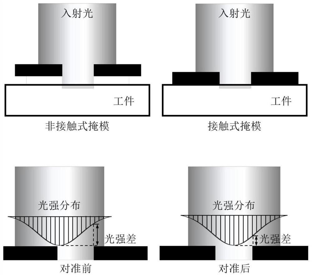

Image

  • Atomic-scale surface and structure ultra-short pulsed light efficient processing method
  • Atomic-scale surface and structure ultra-short pulsed light efficient processing method
  • Atomic-scale surface and structure ultra-short pulsed light efficient processing method

Examples


Embodiment Construction

[0039] The present invention will be described in further detail below through specific examples. The following examples are only descriptive and not restrictive, and the protection scope of the present invention cannot be limited by this.

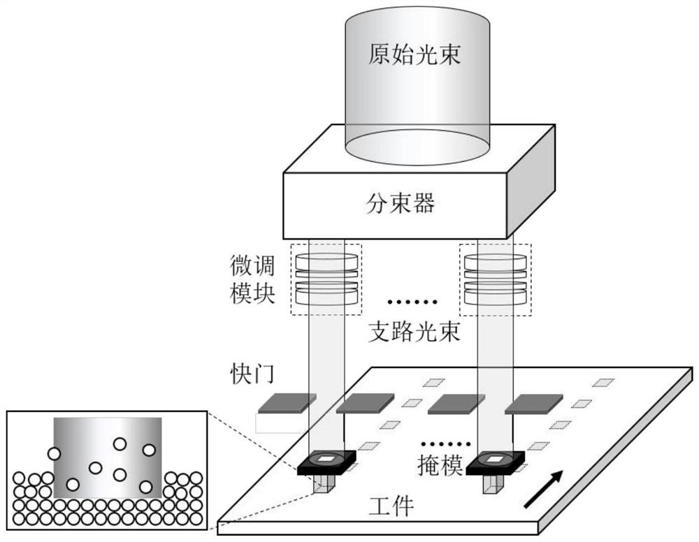
[0040] Combine below figure 2 Taking the surface atomic-level rectangular array processing of monocrystalline silicon (100) as an example, the specific implementation mode is explained:

[0041] 1. Pretreatment of workpiece surface;

[0042] 2. According to the material parameters and the number of atomic layer removal N, the upper limit of wavelength λ is determined by formulas (1) and (2) max And initial value of energy density

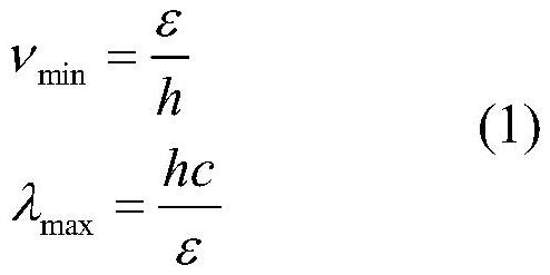
[0043] Assuming that the average chemical bond energy of atoms on the surface of the material is ε, the lower limit of the theoretical frequency of incident light is ν min And the corresponding upper wavelength λ max Respectively

[0044]

[0045] Where h is Planck's constant and c is the speed of light in vacuum. As...


PUM


Abstract

The invention relates to an atomic-scale surface and structure ultra-short pulsed light efficient processing method. Photon energy is used to cut off chemical bonds between atoms on the surface of a material to remove an atomic layer magnitude controllable material in the depth direction. The transverse size precision and the processing uniformity of a to-be-processed structure are guaranteed by aligning a mask with a light beam energy center; and meanwhile, multi-path beam splitting parallel processing is adopted to meet the high-efficiency requirement of large-scale mass production. According to the atomic-scale structure surface processing method based on the optical ultra-short pulse, the light source wavelength is selected in a targeted mode according to physicochemical properties ofthe material to be processed, the limit precision of atomic layer removal is improved, and lattice damage caused by a thermal process is avoided.

Description

Technical field [0001] The invention belongs to the field of Atomic and Near Atomic Scale Manufacturing (ACSM), in particular to a high-efficiency processing method of atomic-level surface and structure ultrashort pulse light. Background technique [0002] Surface structure is the basic element of core devices in the fields of microelectronics and optics. The scale and precision of these structures directly determine the working performance of the device. A typical example is that the number of transistors on integrated circuits doubles every two years (ie Moore’s Law). The number of transistors on a single Intel processor has increased from 2,300 in the 1970s to 1.5 billion in 2015. 1cm 2 6.9 billion components are distributed on the area. On the one hand, the increase in integration has brought a leap in performance, and on the other hand, it means a reduction in the size of the component structure. For example, the line width of integrated circuits has been reduced from the e...

Claims


Application Information

Patent Timeline
Patent Type & Authority Applications(China)
IPC IPC(8): H01L21/027B23K26/36B23K26/362B23K26/402
CPCH01L21/0275B23K26/36B23K26/362B23K26/402
Inventor 房丰洲王金石
Owner TIANJIN UNIV
Learn More