Export design method and device of multi-connector module
A technology of a connector module and a design method, which is applied in the directions of computer design circuits, assembling printed circuits with electrical components, and making wiring diagrams of printed circuits, etc., can solve the problems of complicated patching process and low patching efficiency, and improve patch The effect of working efficiency and ensuring accuracy
- Summary
- Abstract
- Description
- Claims
- Application Information
AI Technical Summary
Problems solved by technology
Method used
Image
Examples
Embodiment 1
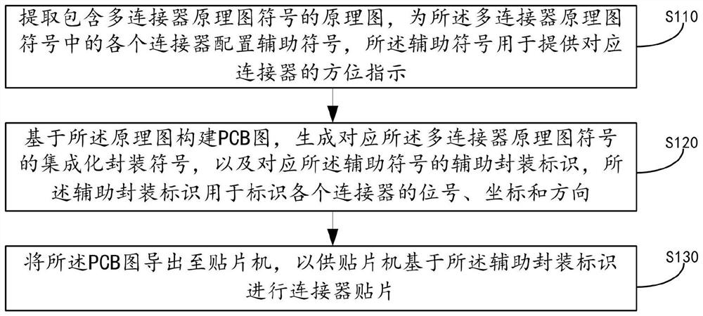
[0042] figure 1 A flowchart of a derivation design method for a multi-connector module provided in Embodiment 1 of the present application is given. The derivation design method for a multi-connector module provided in this embodiment can be executed by a derivation design device for a multi-connector module. The deriving design device of the multi-connector module may be realized by means of software and / or hardware, and the deriving design device of the multi-connector module may be composed of two or more physical entities, or may be composed of one physical entity. Generally speaking, the exporting design equipment of the multi-connector module can be a terminal equipment such as a computer, a PCB schematic diagram drawing platform, and the like.
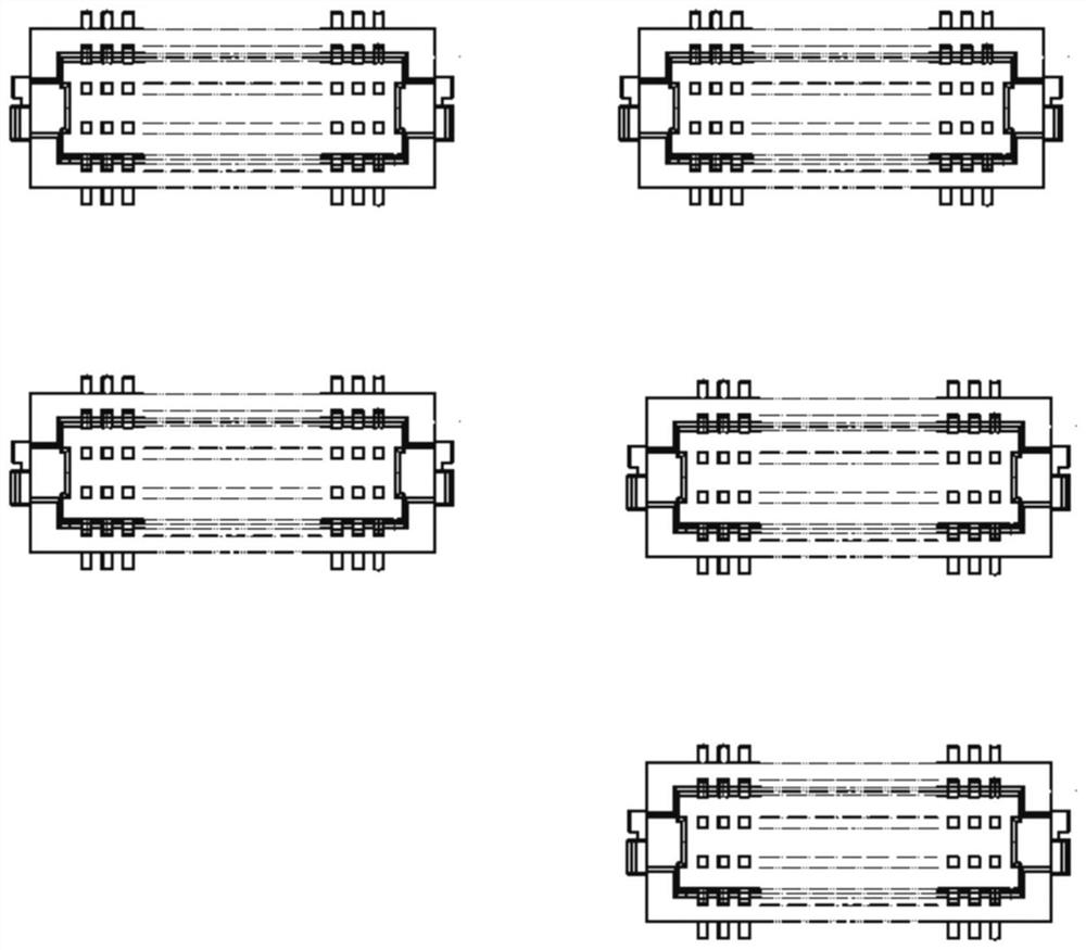
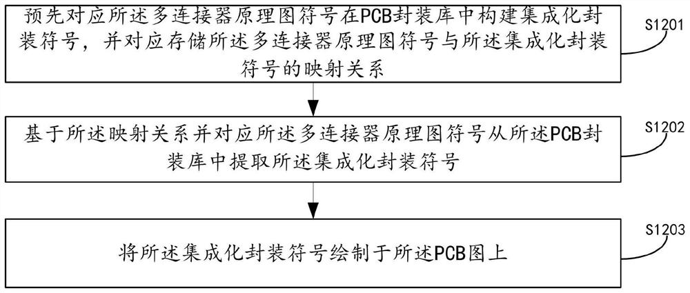
[0043] The following description will be made by taking the derivation design device of the multi-connector module as the main body executing the derivation design method of the multi-connector module as an example. refer to f...
Embodiment 2
[0063] On the basis of the above examples, Figure 5 It is a schematic structural diagram of a device for deriving and designing a multi-connector module provided in Embodiment 2 of the present application. refer to Figure 5 , the export design device for the multi-connector module provided in this embodiment specifically includes: a configuration module 21 , a package module 22 and an export module 23 .
[0064] Wherein, the configuration module 21 is used to extract a schematic diagram containing multi-connector schematic symbols, and configure auxiliary symbols for each connector in the multi-connector schematic symbols, and the auxiliary symbols are used to provide orientation indications for corresponding connectors ;
[0065]The package module 22 is used to construct a PCB diagram based on the schematic diagram, generate an integrated package symbol corresponding to the multi-connector schematic symbol, and an auxiliary package label corresponding to the auxiliary sym...
Embodiment 3
[0070] Embodiment 3 of the present application provides an electronic device, referring to Figure 6 , the electronic device includes: a processor 31 , a memory 32 , a communication module 33 , an input device 34 and an output device 35 . The number of processors in the electronic device may be one or more, and the number of memories in the electronic device may be one or more. The processor, memory, communication module, input device and output device of the electronic device can be connected through a bus or in other ways.
[0071] The memory 32, as a computer-readable storage medium, can be used to store software programs, computer-executable programs and modules, such as the program instructions / modules corresponding to the derivation design method of the multi-connector module described in any embodiment of the present application (for example, Configuration Module, Encapsulation Module, and Export Module in Export Design for Multi-Connector Modules). The memory may mai...
PUM
 Abstract
Description
Claims
Application Information
 - R&D Engineer
- R&D Manager
- IP Professional
- Industry Leading Data Capabilities
- Powerful AI technology
- Patent DNA Extraction
Browse by: Latest US Patents, China's latest patents, Technical Efficacy Thesaurus, Application Domain, Technology Topic, Popular Technical Reports.
© 2024 PatSnap. All rights reserved.Legal|Privacy policy|Modern Slavery Act Transparency Statement|Sitemap|About US| Contact US: help@patsnap.com


