
Brightness compensation method for organic light-emitting diode display panel

A technology of light-emitting diodes and brightness compensation, applied to static indicators, instruments, etc., can solve the problems of decreased aperture ratio, improved OLED life, limited efficiency, and no consideration of display effects, etc.

Inactive Publication Date: 2020-08-18
INCOFLEX SEMICON TECH CO LTD
View PDF10 Cites 8 Cited by
  • Summary
  • Abstract
  • Description
  • Claims
  • Application Information

AI Technical Summary

Problems solved by technology

[0005] With the continuous improvement and perfection of OLED production and packaging technology, it is becoming more and more difficult to improve the life of OLED in terms of technology; internal circuit compensation will increase the number of TFTs and capacitors, which will lead to a decrease in aperture ratio, thus improving OLED life. The efficiency is limited; the improvement of external circuit compensation and image processing methods has infinite possibilities for improving the life of OLEDs. A large number of scholars have concentrated their research. Among them, Kyonghwan Oh et al. proposed an OLED life improvement algorithm based on increasing the duty cycle of OLED luminescence time Combined with digital hardware circuits to realize [5]([5]Kyonghwan Oh,Seong-KwanHongand Oh-Kyong Kwon Lifetime Extension Method for Active MatrixOrganicLight-Emitting Diode Displays Using a Modified Stretched Exponential DecayModel,[J]IEEE Electron Device Letters,VOL. 36, NO.3, March 2015), however, this method is only applicable to digital circuits, and this method does not consider the actual display effect

Method used


Image

  • Brightness compensation method for organic light-emitting diode display panel
  • Brightness compensation method for organic light-emitting diode display panel
  • Brightness compensation method for organic light-emitting diode display panel

Examples


Embodiment Construction

[0063] The detailed description and technical content of the present invention are described below with the accompanying drawings, but the attached drawings are only for reference and illustration, and are not intended to limit the present invention. Various embodiments of the present invention will be described in detail below with reference to the accompanying drawings, but the present invention is not limited to these embodiments. The present invention covers any alternatives, modifications, equivalent methods and schemes made on the spirit and scope of the present invention. In order to provide the public with a thorough understanding of the present invention, specific details are set forth in the following preferred embodiments of the present invention, but those skilled in the art can fully understand the present invention without the description of these details.

[0064] Unless otherwise defined, the technical terms or scientific terms used in the present disclosure sh...


PUM


Abstract

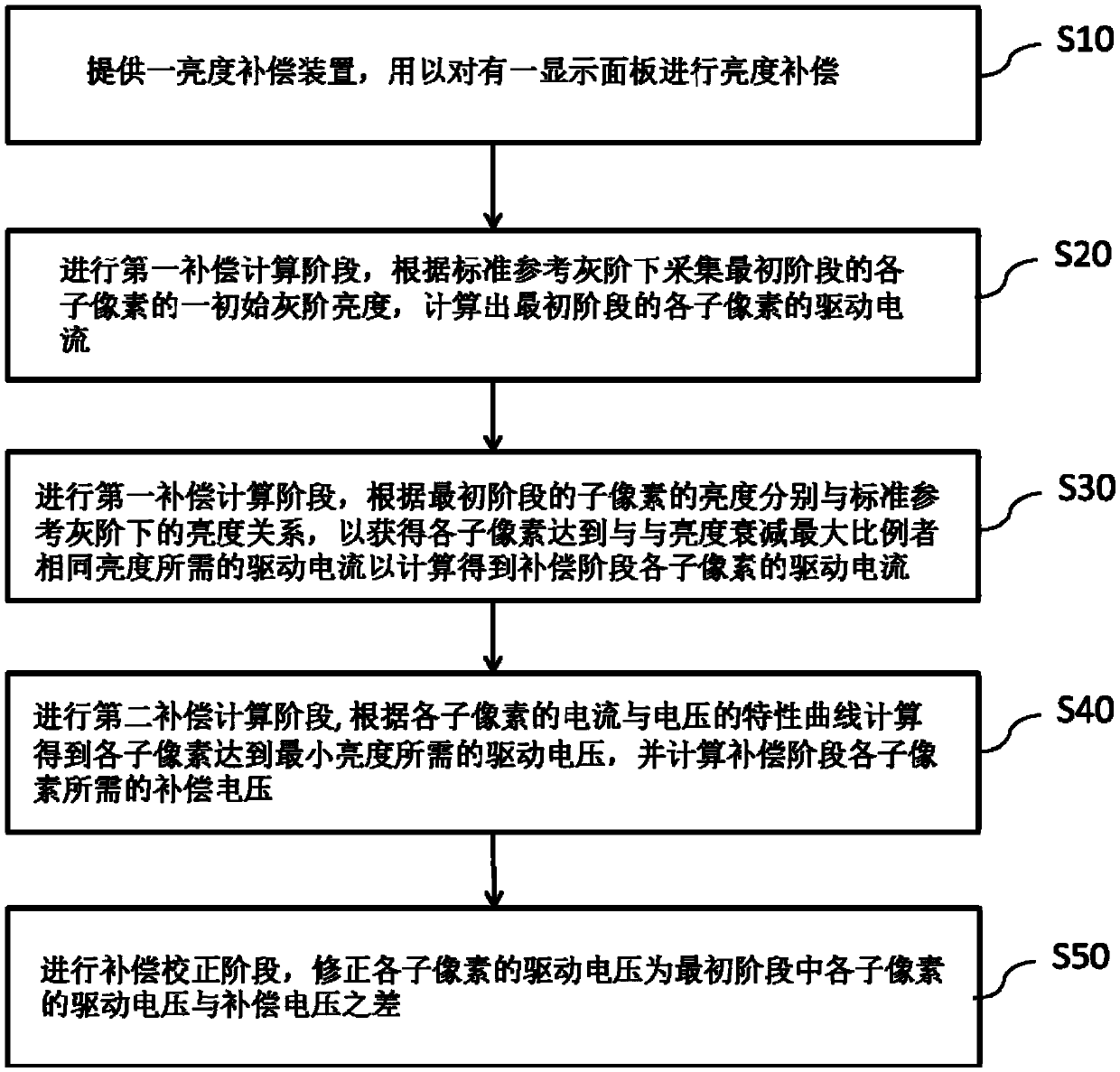
The invention provides a brightness compensation method for an organic light-emitting diode display panel, which comprises the following steps of: performing an initial brightness acquisition stage, separately acquiring an initial gray scale brightness of each sub-pixel in an initial stage, and calculating a driving current of each sub-pixel in the initial stage; performing a first compensation calculation stage, and according to a brightness relationship between the brightness of the sub-pixels in the initial stage and a standard reference gray scale, obtaining a driving current required foreach sub-pixel to reach the same brightness as the initial stage so as to calculate the driving current of each sub-pixel in the compensation stage; performing a second compensation calculation stage,performing calculation according to the characteristic curve of the current and the voltage of each sub-pixel to obtain a driving voltage required by each sub-pixel, and calculating a compensation voltage required by each sub-pixel in the compensation stage; and performing a compensation correction stage, and correcting the driving voltage of each sub-pixel to be the sum of the driving voltage and the compensation voltage of each sub-pixel in the initial stage. Therefore, the branding phenomenon on the display panel is reduced and corrected.

Description

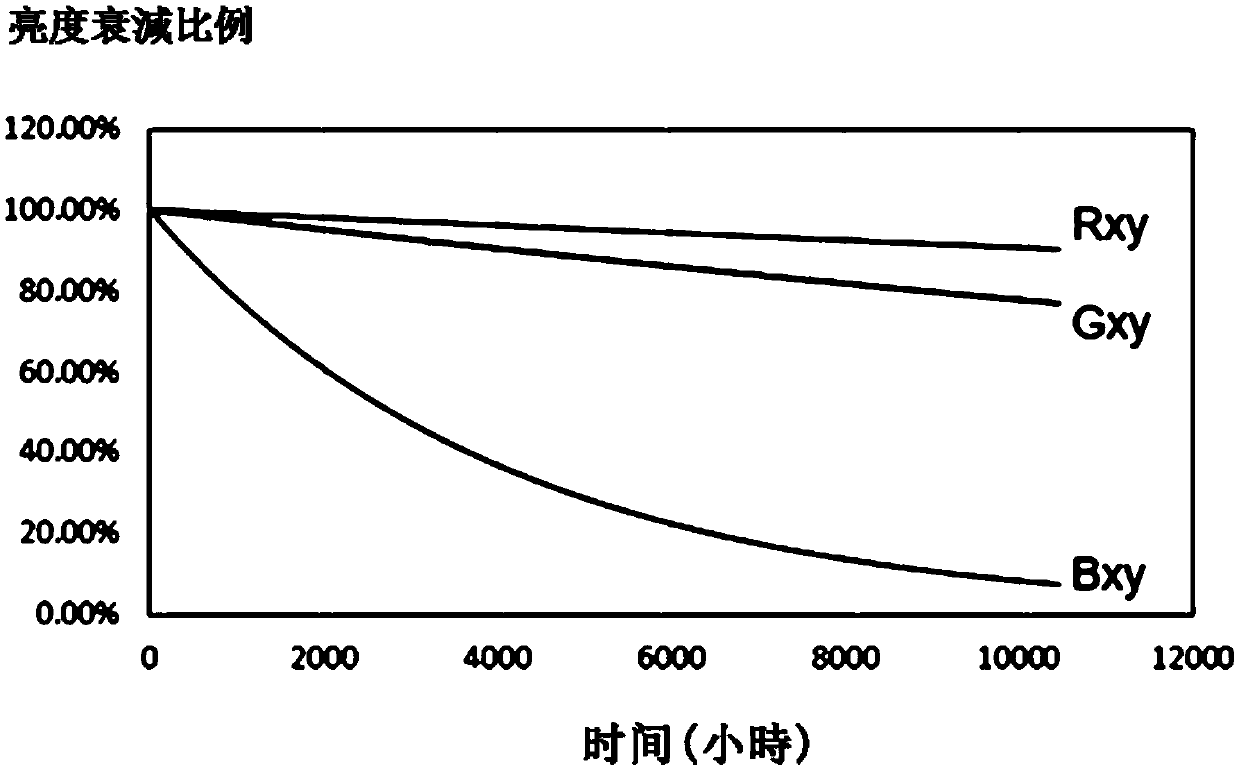
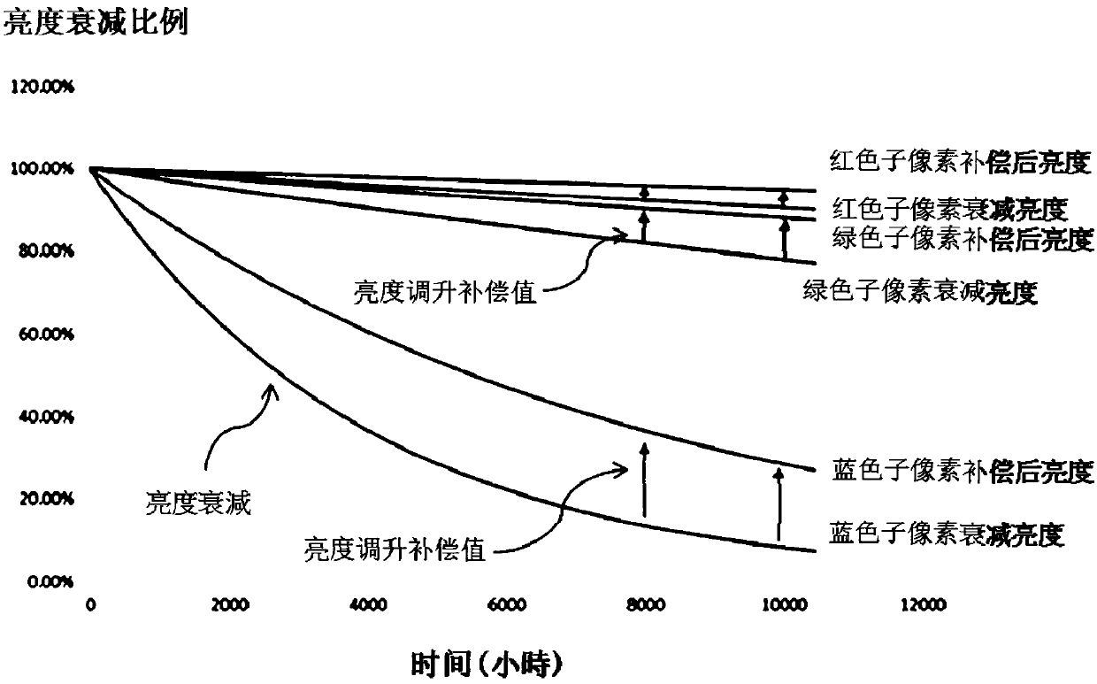
technical field [0001] The present invention relates to the technical field of a display panel, in particular to a method for correcting the brightness attenuation curve of each pixel in the AMOLED according to the brightness attenuation characteristics of an active matrix organic light emitting device (AMOLED), and optimizing the brightness of each pixel in the AMOLED compensation method. Background technique [0002] At present, Organic Light-Emitting Diode (OLED) is an emerging application technology of flat-panel displays. Due to its self-luminous characteristics, no need for backlight, energy saving, and large viewing angle, it has been used in mobile phones, digital cameras, It is widely used in terminals such as tablet PCs and televisions. OLED display devices can be divided into two categories: passive matrix OLED (PMOLED) and active matrix OLED (AMOLED) according to the driving method, namely direct addressing and thin film transistor (Thin Film Transistor, TFT) ma...

Claims


Application Information

Patent Timeline
Patent Type & Authority Applications(China)
IPC IPC(8): G09G3/3233
CPCG09G3/3233G09G2320/0271G09G2320/029G09G2320/0626
Inventor 蔡昆华
Owner INCOFLEX SEMICON TECH CO LTD
Learn More