Semiconductor device and forming method thereof

A technology of semiconductors and devices, which is applied in the field of semiconductor devices and their formation, can solve problems such as complex semiconductor device processes, and achieve the effects of accurate and controllable positions, high precision, and simplified process procedures

Pending Publication Date: 2020-08-07
SEMICON MFG INT (SHANGHAI) CORP +1
View PDF3 Cites 0 Cited by
  • Summary
  • Abstract
  • Description
  • Claims
  • Application Information

AI Technical Summary

Problems solved by technology

[0005] However, the process of forming a semiconductor device with a single diffusion isolation structure in the prior art is complicated

Method used


Image

  • Semiconductor device and forming method thereof
  • Semiconductor device and forming method thereof
  • Semiconductor device and forming method thereof

Examples


Embodiment Construction

[0026] As described in the background, prior art semiconductor devices have poor performance.

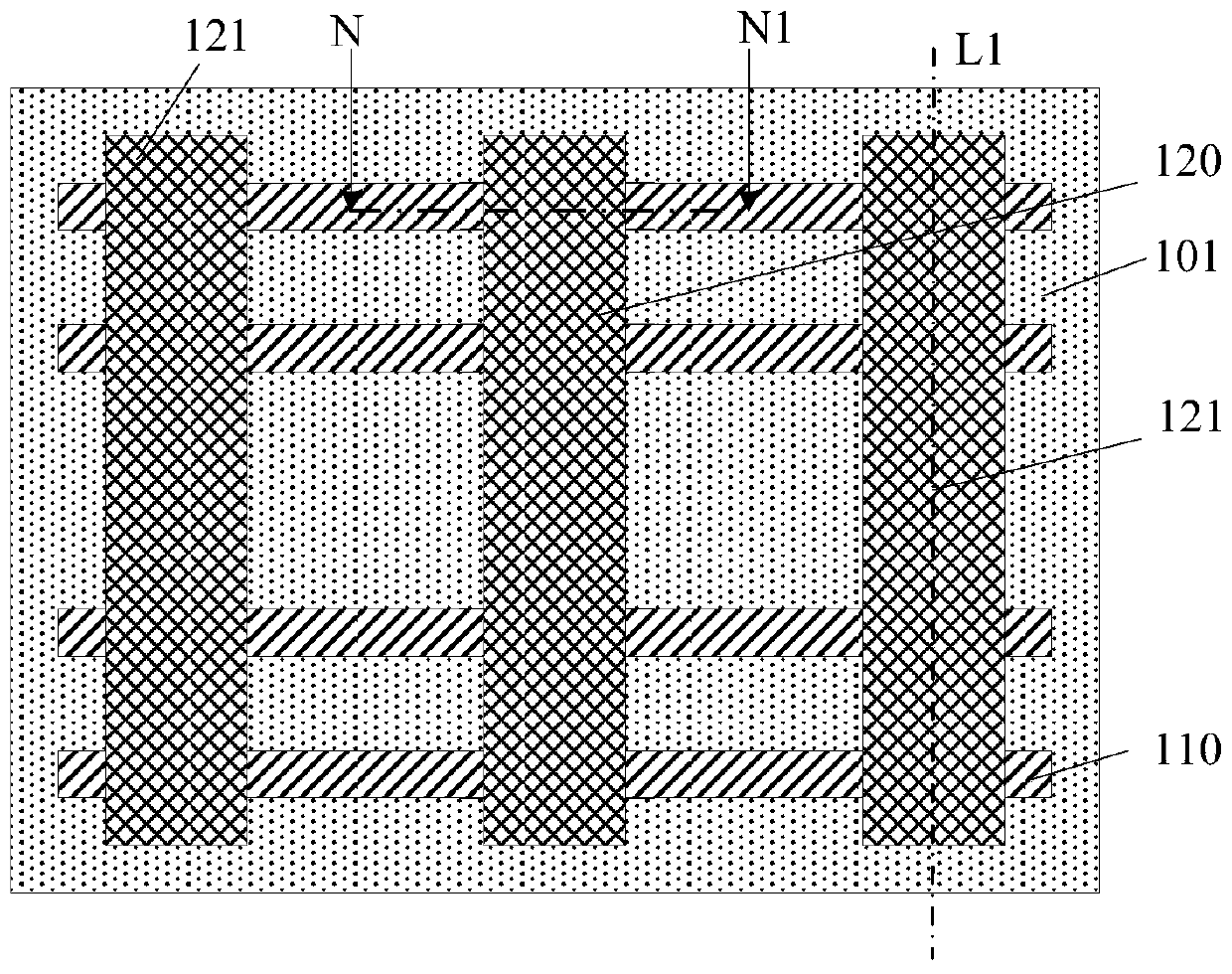
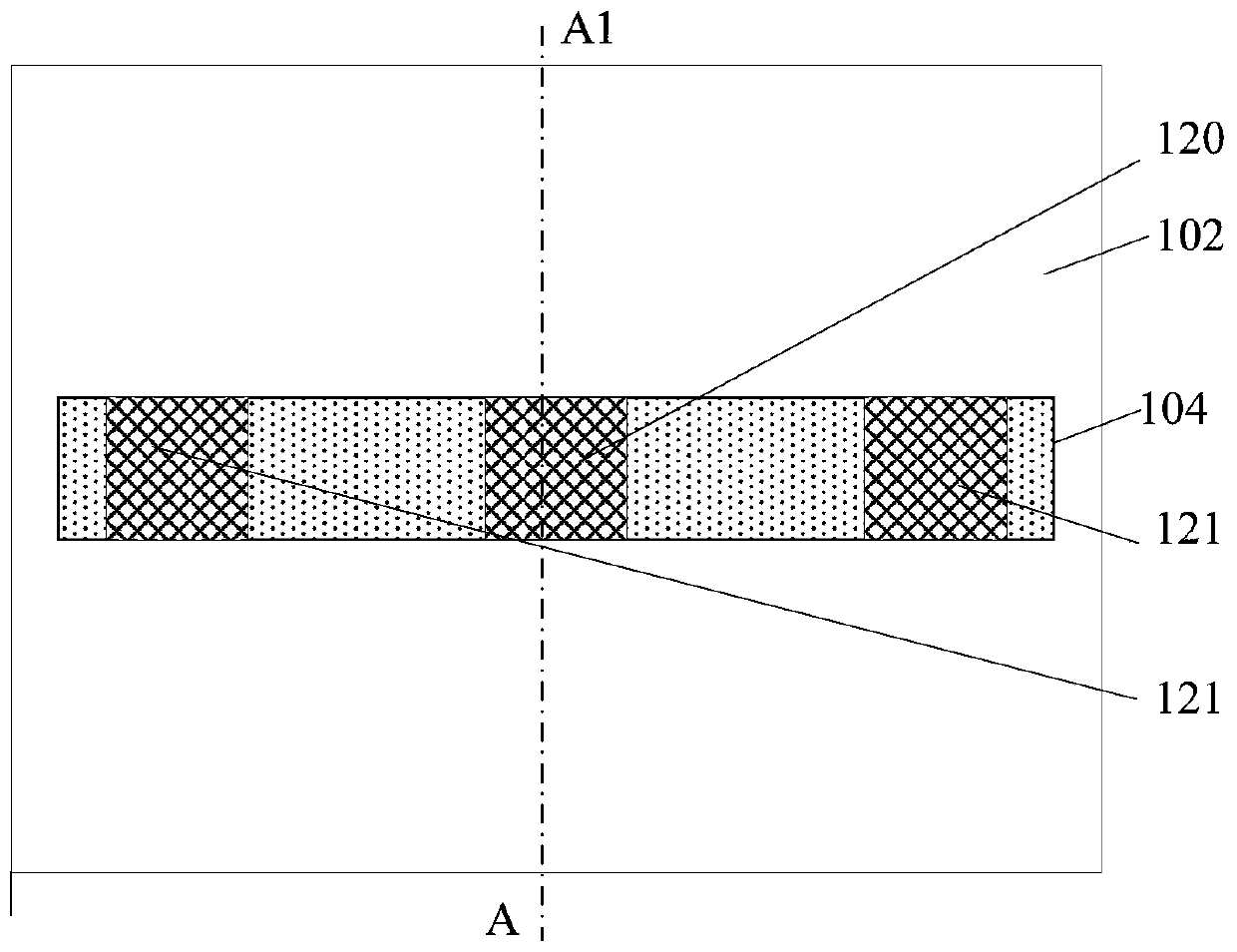
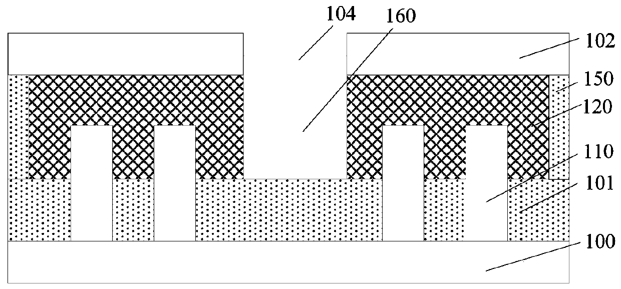
[0027] Figure 1 to Figure 5 It is a structural schematic diagram of the formation process of a semiconductor device.

[0028] refer to figure 1 , figure 1 As a top view of a semiconductor device, a semiconductor substrate 100 is provided; a plurality of fins 110 are formed on the semiconductor substrate 100, and the extending direction of the fins 110 is a first direction; an isolation structure 101 is formed on the semiconductor substrate 100 ; forming a sacrificial gate structure 120 and a gate structure 121 across the plurality of fins 110 on the isolation structure 101, the extension direction of the gate structure 121 being the second direction; forming the gate structure 121 and the sacrificial gate structure After 120 , a source-drain doped layer 140 is formed in the fins 210 on both sides of the gate structure 121 and on both sides of the sacrificial gate structure 120 ...


PUM

PropertyMeasurementUnit
Depthaaaaaaaaaa

Abstract

The invention discloses a semiconductor device and a forming method thereof. The method comprises the steps: providing a substrate, wherein the substrate comprises a first region, a second region anda third region which are arranged in a first direction; forming a plurality of fin parts arranged in parallel on the substrate, wherein the extending direction of each fin part is parallel to the first direction; forming a sacrificial gate structure and a plurality of gate structures which stretch across the plurality of fin parts, wherein the gate structures are located on the first region and the third region of the substrate, the extension directions of the gate structures are a second direction, and the sacrificial gate structures are located on the second region; forming a dielectric layer on the substrate; forming a mask layer with a first opening and a second opening on the dielectric layer, wherein the first opening is located on the second region to expose the sacrificial gate structure, and the second opening is located on the first region and the third region to expose part of the gate structure; and etching the sacrificial gate structure and the fin part at the bottom of the first opening and part of the gate structure exposed out of the second opening by taking the mask layer as a mask to form a first groove and a second groove respectively. The method improves the performance of the semiconductor device.

Description

technical field [0001] The invention relates to the field of semiconductor manufacturing, in particular to a semiconductor device and a forming method thereof. Background technique [0002] With the rapid development of semiconductor manufacturing technology, semiconductor devices are developing towards higher element density and higher integration. Transistors, as the most basic semiconductor devices, are being widely used at present. The control ability of traditional planar transistors on channel current is weakened, resulting in short channel effect and leakage current, which ultimately affects the electrical performance of semiconductor devices. [0003] The design of three-dimensional structures such as Fin Field Effect Transistor (Fin FET) has become a hot spot in this field. Fin Field Effect Transistor (Fin FET) is an emerging multi-gate device. Fin FET generally has a plurality of thin fins extending vertically upward from the substrate, and the channel of Fin FET ...

Claims


Application Information

Patent Timeline
IPC IPC(8): H01L21/8234H01L27/088
CPCH01L21/823431H01L21/823481H01L27/0886H01L29/66545H01L21/823437H01L21/76224H01L21/3065H01L21/31111H01L21/0337H01L21/32139
Inventor 王楠
Owner SEMICON MFG INT (SHANGHAI) CORP
Why Eureka
Try Eureka