Circuit board hole filling method and circuit board

A circuit board, blind via technology, applied in printed circuits, printed circuit manufacturing, printed circuit secondary processing, etc., can solve problems affecting circuit board reliability, copper breakage, delamination, etc., to achieve tight bonding, reduce breakage, The effect of improving reliability

Active Publication Date: 2020-07-24
SHENNAN CIRCUITS
View PDF5 Cites 0 Cited by
  • Summary
  • Abstract
  • Description
  • Claims
  • Application Information

AI Technical Summary

Problems solved by technology

[0003] The inventors of the present application found in the long-term research and development process that when the thermomechanical load is large, the copper filled in the blind hole may break and delaminate, thereby affecting the reliability of the circuit board

Method used


Image

  • Circuit board hole filling method and circuit board
  • Circuit board hole filling method and circuit board

Examples


Embodiment Construction

[0021] The following will clearly and completely describe the technical solutions in the embodiments of the present application with reference to the drawings in the embodiments of the present application. Obviously, the described embodiments are only some of the embodiments of the present application, not all of them. Based on the embodiments in this application, all other embodiments obtained by persons of ordinary skill in the art without making creative efforts belong to the scope of protection of this application.

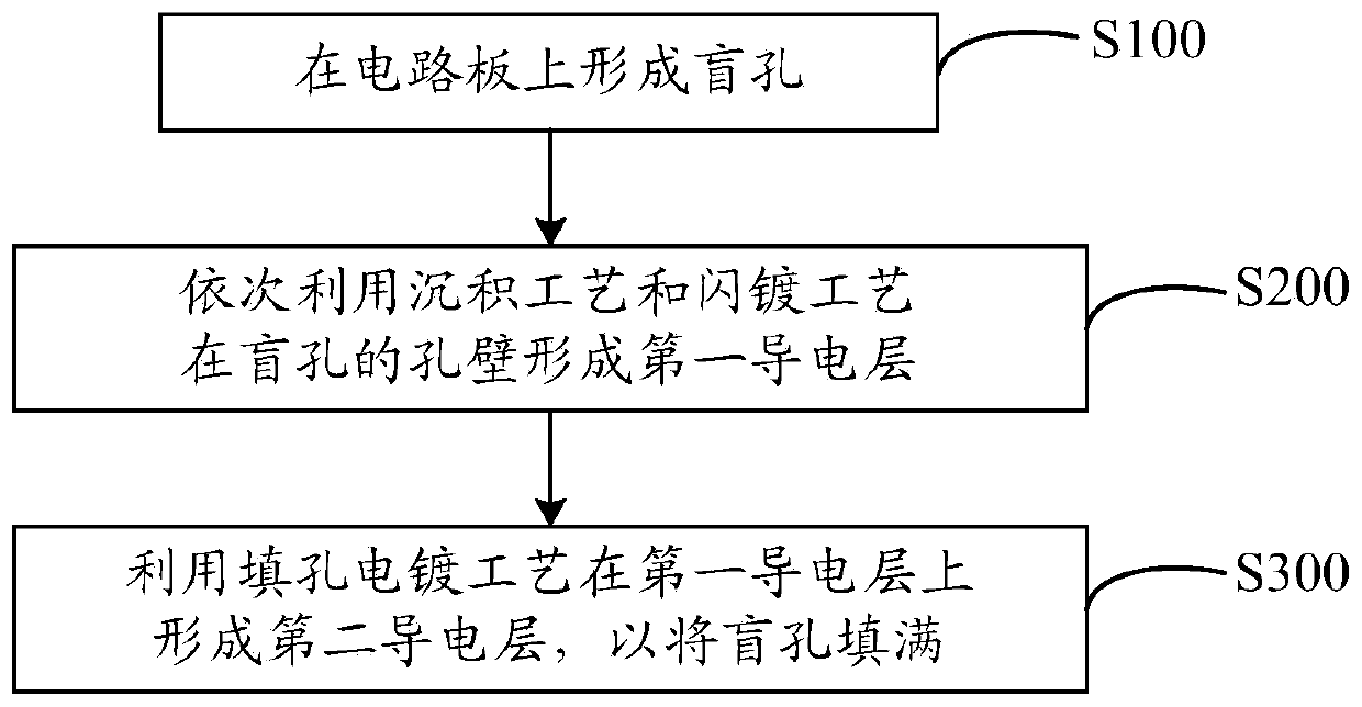
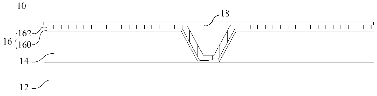
[0022] see figure 1 , figure 1 It is a schematic flow chart of an embodiment of the circuit board hole filling method of the present application. For ease of understanding, please refer to figure 2 , figure 2 It is a schematic cross-sectional view of an embodiment of the circuit board of the present application. Wherein, the cross-sectional schematic diagram is only schematic and has been enlarged. The circuit board 10 includes an inner plate 12, a surfac...


PUM


Abstract

The invention discloses a circuit board hole filling method and a circuit board. The circuit board hole filling method comprises the steps of forming blind holes in the circuit board; forming a firstconductive layer on the hole wall of the blind hole by using a deposition process and a flash plating process in sequence, wherein the volume of the blind hole is greater than that of the first conductive layer; and forming a second conductive layer on the first conductive layer by using a hole filling electroplating process to fill the blind hole, wherein the hole filling electroplating process comprises a pre-plating process and an electroplating process which are carried out in sequence, the current density of the pre-plating process is smaller than the current density of the electroplatingprocess, and the time of the pre-plating process is less than the time of the electroplating process. By means of the mode, the bonding force between the first conductive layer and the second conductive layer can be improved, the probability that the first conductive layer and the second conductive layer are broken and layered when a thermo-mechanical load is large is reduced, and then the reliability of the circuit board is improved.

Description

technical field [0001] The present application relates to the technical field of circuit boards, in particular to a circuit board hole filling method and a circuit board. Background technique [0002] With the vigorous development of the electronic industry, the application of circuit boards is becoming more and more extensive, and the requirements for its functions are becoming more and more abundant. In order to meet more powerful functional requirements, circuit boards usually include multi-layer laminated boards. Blind holes are usually opened between the surface board and the inner board, and conductive materials, such as copper, are filled in the blind holes. [0003] The inventors of the present application have found in the long-term research and development process that when the thermomechanical load is large, the copper filled in the blind hole may break and delaminate, thereby affecting the reliability of the circuit board. Contents of the invention [0004] Th...

Claims


Application Information

Patent Timeline
Patent Type & Authority Applications(China)
IPC IPC(8): H05K3/42H05K3/24
CPCH05K3/241H05K3/421H05K3/424
Inventor 杨之诚曹权根
Owner SHENNAN CIRCUITS
Why Eureka
Try Eureka