


Quick Research
Generate reliable direction feasibility study reports for your R&D in just a few steps.

Technical Q&A
Discover and master advanced knowledge NOW. Basics, ideas, possibilities, all at once.

Find Solutions
As an expert in R&D theories, this can generate solutions to your technical problems instantly.

Evaluate Feasibility
Analyze your overall solution with one click, know your potential R&D risks in advance.

Monitor Landscape
Get weekly tech updates, stay abreast of the latest tech innovations and key insights.
Composite material, quantum dot light emitting diode and preparation method thereof
A quantum dot light-emitting and composite material technology, applied in the field of quantum dot light-emitting devices, can solve the problems of difficult and complicated development
- Summary
- Abstract
- Description
- Claims
- Application Information
AI Technical Summary
Problems solved by technology
Method used
Image

Examples
Embodiment 1
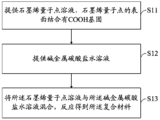
[0068] The preparation steps of the composite material are as follows:
[0069] 2.5g of carbon black was added to a mixture of 100ml of concentrated sulfuric acid and 50ml of concentrated nitric acid, heated and stirred for 24 hours;
[0070] After the solution is cooled, add deionized water to dilute, and adjust the acidity of the solution to PH=1;
[0071] Adding excess acetone, removing the precipitate, and distilling the remaining solution to obtain a solid, which is the graphene quantum dot;
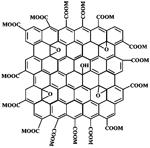
[0072] Dissolving the graphene quantum dot solid in an aqueous solvent with a concentration of 10mg / ml; and preparing an aqueous solution of alkali metal carbonate in advance with a concentration of 20mg / ml;
[0073] Gradually add an aqueous alkali metal carbonate solution to the graphene quantum dot solution until the pH value of the solution reaches 7.
[0074] The above solution is distilled to obtain a solid, which is a composite material.
Embodiment 2
[0076] The preparation steps of the formal structure light-emitting diode are as follows:
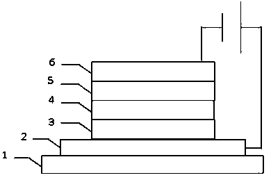
[0077] Use transparent conductive film ITO as the anode, 50nm thick;
[0078] In the air environment, deposit PEDOT:PSS on the anode as a hole injection layer by solution method, with a thickness of 30nm, and anneal in air at 150°C for 10 minutes;
[0079] In a nitrogen environment, deposit TFB on the hole injection layer as a hole transport layer by solution method, with a thickness of 30nm, and anneal at 150°C for 30 minutes in a nitrogen environment;
[0080] In a nitrogen environment, deposit CdSe / ZnS as a quantum dot light-emitting layer on the hole transport layer by solution method, with a thickness of 25nm, and anneal at 80°C for 30 minutes in a nitrogen environment;
[0081] In a nitrogen environment, use a solution method to deposit graphene quantum dots bound to the surface of cesium on the quantum dot light-emitting layer as an electron transport layer, with a thickness of ...
Embodiment 3
[0084] The preparation steps of the trans-structure light-emitting diode are as follows:
[0085] Use transparent conductive film ITO as the cathode, 50nm thick;
[0086] In a nitrogen environment, use a solution method to deposit graphene quantum dots bound to the surface of cesium on the cathode as an electron transport layer, with a thickness of 40nm, and anneal at 70°C for 20 minutes in a nitrogen environment;
[0087] In a nitrogen environment, deposit CdSe / ZnS as a quantum dot light-emitting layer on the electron transport layer by solution method, with a thickness of 25nm, and anneal at 80°C for 30 minutes in a nitrogen environment;
[0088] Transfer the substrate to the evaporation chamber and vacuum to 10 -5 Pa level, TCTA is vapor deposited on the quantum dot light-emitting layer as a hole transport layer, with a thickness of 40nm;
[0089] Evaporate and deposit HAT-CN on the hole transport layer as a hole injection layer, 10nm thick;
[0090] Al was evaporated on...
PUM
 Abstract
Description
Claims
Application Information
 - R&D Engineer
- R&D Manager
- IP Professional
- Industry Leading Data Capabilities
- Powerful AI technology
- Patent DNA Extraction
Browse by: Latest US Patents, China's latest patents, Technical Efficacy Thesaurus, Application Domain, Technology Topic, Popular Technical Reports.
© 2024 PatSnap. All rights reserved.Legal|Privacy policy|Modern Slavery Act Transparency Statement|Sitemap|About US| Contact US: help@patsnap.com