Microscopic imaging system

A microscopic imaging and image processing technology, applied in the field of optical imaging, can solve the problems of unevenness, clear imaging, and the problem of focusing is not well solved, and achieves the effect of reducing the requirement of consistency and improving the production efficiency of finished products.

Inactive Publication Date: 2020-06-26
CONVERGENCE TECH CO LTD
View PDF6 Cites 2 Cited by
  • Summary
  • Abstract
  • Description
  • Claims
  • Application Information

AI Technical Summary

Problems solved by technology

Moreover, for some samples with large undulations, such as stacked cell samples, the sample itself has unevenness, even if the array imaging system has reached the parfocal design, it cannot complete the alignment in a single imaging process. Clear imaging of such samples
It can be seen that due to the large size of the traditional microscope eyepiece body relative to the sample, and there is no adjustable focus microscopic microscope product or combination method suitable for this situation, in the existing technical solutions, this type of focusing problem has not been solved. good solution

Method used


Image

  • Microscopic imaging system
  • Microscopic imaging system
  • Microscopic imaging system

Examples


Embodiment 1

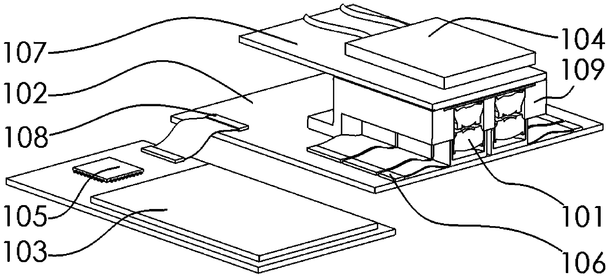
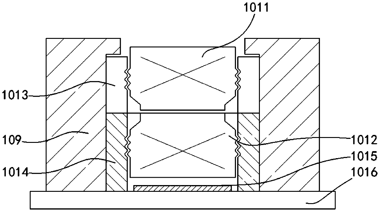
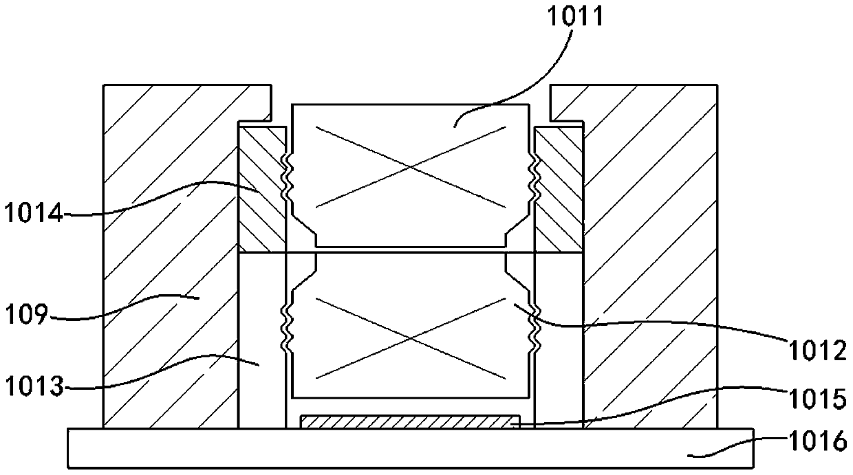
[0071] Such as figure 1 As shown, in this embodiment, the microscopic imaging system includes six unit microscopic imaging modules 101, the six unit microscopic imaging modules 101 are arranged in an array structure with the minimum physical distance, and are fixed by a fixing mechanism 109 On the data acquisition card 102. The six unit microscopic imaging modules 101 are respectively connected to the data acquisition card 102 through the board cable interface 106 . Above the unit microscopic imaging module 101, a carrying platform ( figure 1 not shown), the sample 107 to be tested can be set on the carrying platform. At the same time, an illumination source 104 is provided above the carrying platform. The data acquisition card 102 is provided with six independent image processing chips ( figure 1 not shown) independently control the photosensitive modules and focus motors 1013 in the six unit microscopic imaging modules 101 ( figure 1 not shown). The image processing ch...

Embodiment 2

[0076] Such as Figure 5 As shown, on the basis of Embodiment 1, the illumination light source provided above the carrying platform is a fluorescence excitation light source, and the fluorescence excitation light source can use an oblique incident laser 1041 . It can use a 488nm wavelength laser. When a fluorescence excitation light source is used, a corresponding fluorescence excitation filter 302 is added to each unit microscopic imaging module 101 .

Embodiment 3

[0078] Such as Image 6 As shown, on the basis of Embodiment 1, the illumination light source provided above the carrying platform is a fluorescent light source, and the fluorescent excitation light source can use an LED light emitting chip 1042 . It can use LED light-emitting chips with a wavelength of 488nm. When a fluorescence excitation light source is used, a corresponding fluorescence excitation filter 302 is added to each unit microscopic imaging module 101 .

[0079] Figure 7 to Figure 9 for Figure 5 with Image 6 Different embodiments of the unit microscopic imaging module 101 in the illustrated embodiment.

[0080] Such as Figure 7 As shown, in this embodiment, the fluorescence excitation filter 302 is located between the first lens group 1011 and the sample 107 in the unit microscope imaging module 101 . Such as Figure 8 As shown, in this embodiment, the fluorescence excitation filter 302 is located between the first lens group 1011 and the second lens gr...


PUM


Abstract

The invention relates to a microscopic imaging system. The microscopic imaging system comprises a plurality of unit microscopic imaging modules arranged according to a preset rule, and a data collection card connected with the plurality of unit microscopic imaging modules, wherein each unit microscopic imaging module comprises an adjustable lens group capable of independently adjusting focusing, and a photosensitive module corresponding to the adjustable lens group; the data collection card is provided with a plurality of image processing modules in one-to-one correspondence with the pluralityof unit microscopic imaging modules. Each image processing module independently controls the focusing of the corresponding adjustable lens group, and obtains the data of the corresponding photosensitive module. By implementing the invention, the consistency requirement of unit module assembly can be reduced, and the production efficiency of finished products is improved.

Description

technical field [0001] The invention relates to the technical field of optical imaging, and more specifically, to a microscopic imaging system. Background technique [0002] With the development of optical imaging technology, the application field of optical imaging module is more and more extensive, and there are more and more products in the field of ultra-macro imaging and microscopic imaging. With the application and development of artificial intelligence technology in the field of image processing and With the mass production of high-performance image processing hardware, microscopic imaging technology is developing in the direction of large field of view, high resolution, and high throughput. For example, in wafer inspection technology in the field of industrial inspection, and cervical screening technology in the field of cancer screening, it is usually necessary to image centimeter-level samples with sub-micron resolution. At the same time, with the development of m...

Claims


Application Information

Patent Timeline
IPC IPC(8): G02B21/36G02B21/24G02B21/10
CPCG02B21/10G02B21/241G02B21/361G02B21/367
Inventor 胡庆磊黄凯李宁李梦婷丁昶杰
Owner CONVERGENCE TECH CO LTD
Why Eureka
Try Eureka