
A lateral high voltage power semiconductor device

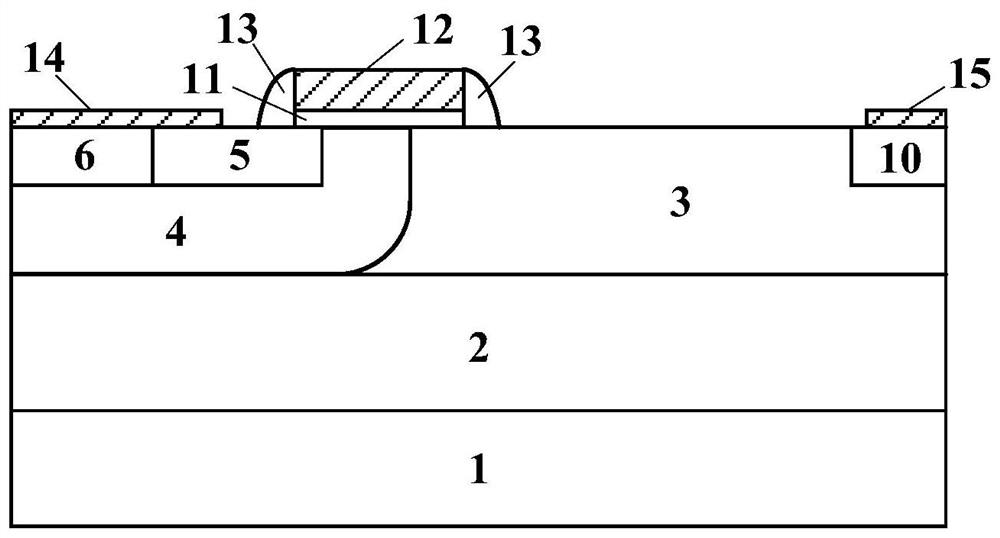
A power semiconductor, lateral high voltage technology, applied in the direction of semiconductor devices, electrical components, circuits, etc., can solve the problems of lower device specific on-resistance, lower device specific on-resistance, and consumption, etc., to achieve lower specific on-resistance, The effect of reducing the area and maintaining the same breakdown voltage

Active Publication Date: 2021-09-07
UNIV OF ELECTRONICS SCI & TECH OF CHINA
View PDF0 Cites 0 Cited by
  • Summary
  • Abstract
  • Description
  • Claims
  • Application Information

AI Technical Summary

Problems solved by technology

The existence of the no-current region means that the electron flow does not fully flow through the entire drift region, and the depletion of the no-current region when the device is blocked will consume the P-type substrate or P-type epitaxial layer used to flow through the drift region. The acceptor charge for charge balance in the region is not conducive to the reduction of the specific on-resistance of the device
If an effective method can be found to make full use of the charge balance to eliminate the no-current region and keep the breakdown voltage constant, the specific on-resistance of the device will be effectively reduced

Method used


Image

  • A lateral high voltage power semiconductor device
  • A lateral high voltage power semiconductor device
  • A lateral high voltage power semiconductor device

Examples


Embodiment 1

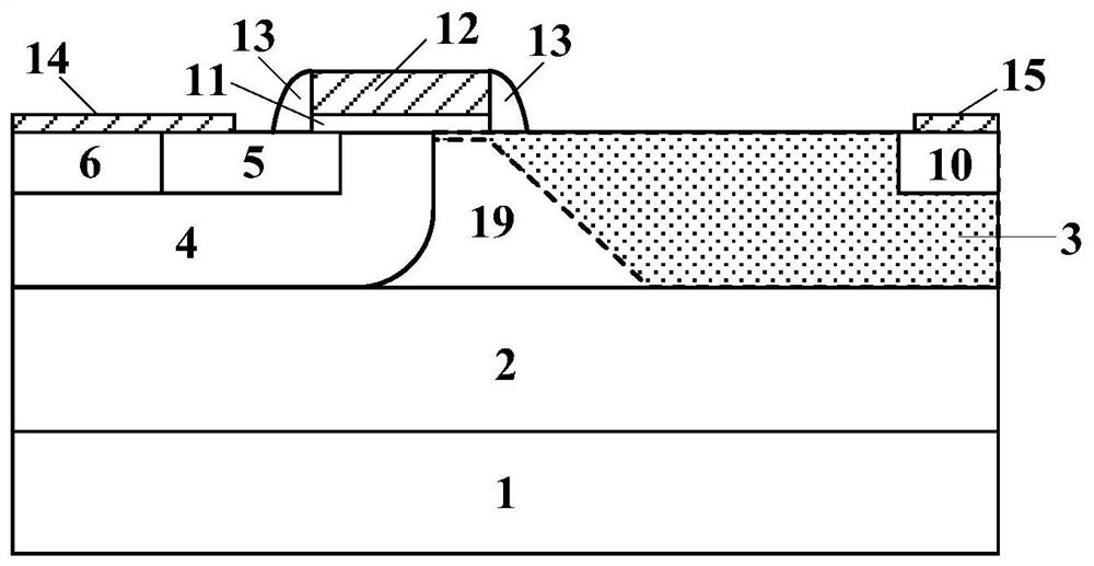
[0033] like figure 2 As shown, this embodiment provides a lateral high-voltage power semiconductor device, including: a P-type substrate 1, a P-type epitaxial layer 2 located above the P-type substrate 1, and an N-type drift layer located on the right side of the P-type epitaxial layer 2. Region 3, the P-type well region 4 located on the left side of the P-type epitaxial layer 2, the first P-type heavily doped region 6 located on the left side of the P-type well region 4, and the first P-type heavily doped region 6 located on the right side of the P-type well region 4. An N-type heavily doped region 5, a first P-type doped region 7 located in the middle of the P-type epitaxial layer 2, a first N-type doped region 8 located on the left side of the N-type drift region 3, and a first N-type doped region 8 located in the N-type drift region. The second N-type doped region 9 in the middle of the region 3, the second N-type heavily doped region 10 located on the right side of the N-...

Embodiment 2

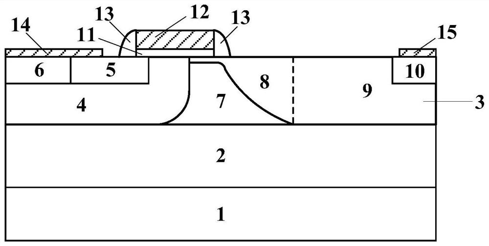
[0041] like image 3 As shown, the present invention is basically the same as Embodiment 1, except that the first P-type doped region 7 is divided into the first P strip 71 to the nth P strip 7n from left to right, where n is greater than or equal to 2. The first N-type doped region 8 is divided into a first N-th strip 81 to an n-th N-th strip 8n from left to right, where n is greater than or equal to 2.

[0042] The first P bar 71 corresponds horizontally to the first N bar 81 and has the same horizontal length, .

[0043] The doping concentration and width of the above regions are respectively adjusted to ensure charge balance, so that the device obtains the minimum specific on-resistance.

Embodiment 3

[0045] like Figure 4 As shown, the present invention is basically the same as Embodiment 1, the difference is that the first N-type doped region 8 is divided into the first N-th strip 81 to the n-th N-th strip 8n from left to right, wherein n is greater than or equal to 2, and the first P Type doped region 7 is not partitioned. Since the thickness of the first P-type doped region gradually decreases from left to right, and the areas of the first N strips 81, ..., nth N strips 8n increase, so in order to ensure charge balance, the first N strips 81, ..., The doping concentration of the nth N-th bar 8n decreases gradually.


PUM


Abstract

The present invention provides a lateral high-voltage power semiconductor device, comprising: a P-type substrate, a P-type epitaxial layer; the P-type epitaxial layer includes a first P-type doped region, an N-type drift region, a P-type well region, a gate oxide layer, Polysilicon gate, sidewall; P-type well region includes first N-type heavily doped region, first P-type heavily doped region; N-type drift region includes first N-type doped region, second N-type doped region 1. The second N-type heavily doped region; the metal cathode covers the surfaces of the first N-type heavily doped region and the first P-type heavily doped region, and the metal anode covers the surface of the second N-type heavily doped region. The invention makes full use of the principle of charge balance, introduces the first P-type doped region to fill the no-current region of the N-type drift region, improves the current conduction path, increases the amount of acceptor charges, and reduces the area of ​​the first N-type doped region , thereby increasing the doping concentration of the first N-type doping region, and reducing the specific on-resistance of the device while keeping the breakdown voltage constant.

Description

technical field [0001] The invention belongs to the technical field of semiconductor power devices, and in particular relates to a lateral high-voltage power semiconductor device. Background technique [0002] Lateral Double-diffused Metal-Oxide-Semiconductor Field Effect Transistor (LDMOSFET), as the core device in Power Integrated Circuit (PIC), has the advantages of easy integration and low driving power. , negative temperature coefficient and other advantages, it has been moving towards high breakdown voltage (Breakdown Voltage, BV) and low specific on-resistance (SpecificOn-Resistance, R for many years) on,sp ) in the direction of development. A higher breakdown voltage requires a device with a longer drift region length and a lower drift region doping concentration, which results in a device with a higher on-resistance. The use of RESURF (reduced surface electric field) technology can improve the constraint relationship between breakdown voltage and on-resistance, an...

Claims


Application Information

Patent Timeline
Patent Type & Authority Patents(China)
IPC IPC(8): H01L29/06H01L29/78H01L29/739
CPCH01L29/0684H01L29/7393H01L29/7816
Inventor 乔明江逸洵冯骏波张波
Owner UNIV OF ELECTRONICS SCI & TECH OF CHINA
Learn More