Active MOSFET voltage clamping circuit, clamping method and double-pulse test circuit

A voltage clamping and voltage clamping technology, applied in the field of voltage clamping measurement modules, can solve the problems of numerous components, temperature sensitivity, complex structure, etc., and achieve the effect of suppressing voltage spikes, widening the voltage measurement range, and improving passive networks

Pending Publication Date: 2020-06-09
HKUST SHENZHEN RES INST
View PDF2 Cites 9 Cited by
  • Summary
  • Abstract
  • Description
  • Claims
  • Application Information

AI Technical Summary

Problems solved by technology

Another object of the present invention is to provide an active MOSFET voltage clamping circuit for the dynamic resistance characterization of commercial p-GaN ga...

Method used


Image

  • Active MOSFET voltage clamping circuit, clamping method and double-pulse test circuit
  • Active MOSFET voltage clamping circuit, clamping method and double-pulse test circuit
  • Active MOSFET voltage clamping circuit, clamping method and double-pulse test circuit

Examples


Embodiment Construction

[0042] The present invention will be further detailed below in conjunction with the accompanying drawings:

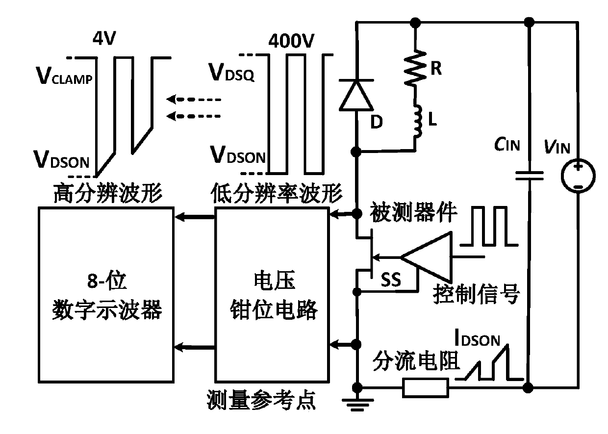
[0043] See figure 2 As shown, the double pulse test circuit includes a device under test (DUT), a shunt resistor R shunt , DC power supply V IN , Capacitance C IN , Inductance L, Schottky diode D SBD Connect the voltage clamp module and the oscilloscope in parallel with the voltage clamp circuit, the oscilloscope, the drain-source of the device under test (DUT), and connect the shunt resistor R to the drain of the device under test (DUT) shunt Connect to ground, shunt resistance R shunt Parallel capacitance C between the other end of and the source of the device under test (DUT) IN And the DC power supply, the inductance L and Schottky diode D are associated between the source of the device under test (DUT) and the parallel capacitor CIN and the common terminal of the DC power supply SBD ; The double pulse test circuit is used to evaluate the switching speed and swit...


PUM


Abstract

The invention relates to an active MOSFET voltage clamping circuit, a clamping method and a double-pulse test circuit. The voltage clamping circuit comprises a device under test, a drain electrode ofthe device under test is connected with a drain electrode of an active clamping tube, a source electrode of the active clamping tube is connected with a clamping end X node, a source electrode of thedevice under test is connected with a Y node of a clamping end, a capacitor C1, a resistor R1 and a Zener diode D2 are connected in parallel between the X node and the Y node by a diode D1. A capacitor C2, a resistor Rg and a power supply (Vcc) are connected in parallel between a grid electrode of the active clamping tube and the common end of the source electrode of the device under test and theY node of the clamping end; a fixed gate bias (Vcc) is applied to the grid electrode of the active clamping tube, when the device under test is in an off state, a voltage VXY between the clamping endnode X and the clamping end node Y is clamped near Vcc-VTH and MT, and when the device under test is in an on state, the voltage VXY follows a conduction voltage VDSON.

Description

Technical field [0001] The invention relates to the technical field of voltage clamping measurement modules for high-voltage power devices, and in particular to an active MOSFET voltage clamping circuit, a clamping method and a double-pulse test circuit for the dynamic resistance characterization of commercial p-GaN gate power devices. Background technique [0002] Commercial p-GaN gate GaN high-voltage devices have the problem of dynamic resistance degradation during high-voltage switching. The huge drain-source voltage swing makes it difficult to accurately monitor the dynamic on-voltage, which affects the evaluation of the dynamic resistance of the p-GaN gate high-voltage device. The dynamic on-resistance can be characterized by dividing the dynamic on-voltage by the dynamic on-current, and the dynamic on-current can be accurately monitored by the shunt resistance. The dynamic turn-on voltage needs to be measured by a voltage clamp module. [0003] The current voltage clamping...

Claims


Application Information

Patent Timeline
IPC IPC(8): G01R31/26G01R27/08G01R1/20G05F1/565G05F1/567G01R15/14G01R15/16
CPCG01R1/20G01R15/146G01R15/16G01R27/08G01R31/2637G05F1/565G05F1/567
Inventor 陈敬钟凯伦
Owner HKUST SHENZHEN RES INST
Why Eureka
Try Eureka