Three-node fault-tolerant stack type D latch for low-power-consumption circuit application

A latch and three-node technology, applied in the direction of reducing power consumption, logic circuits, field effect transistors, etc., can solve problems such as large area, multiple hardware, and large number of sensitive nodes

Inactive Publication Date: 2020-05-22
QIQIHAR UNIVERSITY
View PDF0 Cites 1 Cited by
  • Summary
  • Abstract
  • Description
  • Claims
  • Application Information

AI Technical Summary

Problems solved by technology

[0005] The present invention aims to solve the problems that the traditional anti-three-node flipping D latch needs more hardware, high power consumption, large area and large number of sensitive nodes. Node Fault Tolerant Stacked D-Latch

Method used


Image

  • Three-node fault-tolerant stack type D latch for low-power-consumption circuit application
  • Three-node fault-tolerant stack type D latch for low-power-consumption circuit application

Examples


Embodiment Construction

[0058] The following will clearly and completely describe the technical solutions in the embodiments of the present invention with reference to the accompanying drawings in the embodiments of the present invention. Obviously, the described embodiments are only some, not all, embodiments of the present invention. Based on the embodiments of the present invention, all other embodiments obtained by persons of ordinary skill in the art without making creative efforts belong to the protection scope of the present invention.

[0059] It should be noted that, in the case of no conflict, the embodiments of the present invention and the features in the embodiments can be combined with each other.

[0060] The present invention will be further described below in conjunction with the accompanying drawings and specific embodiments, but not as a limitation of the present invention.

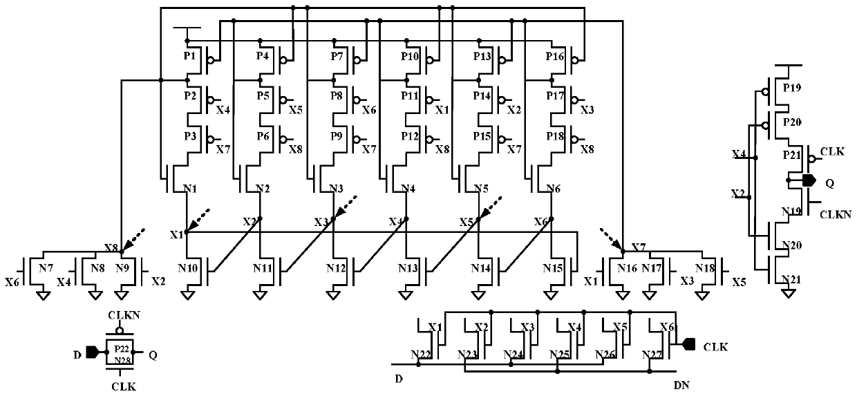
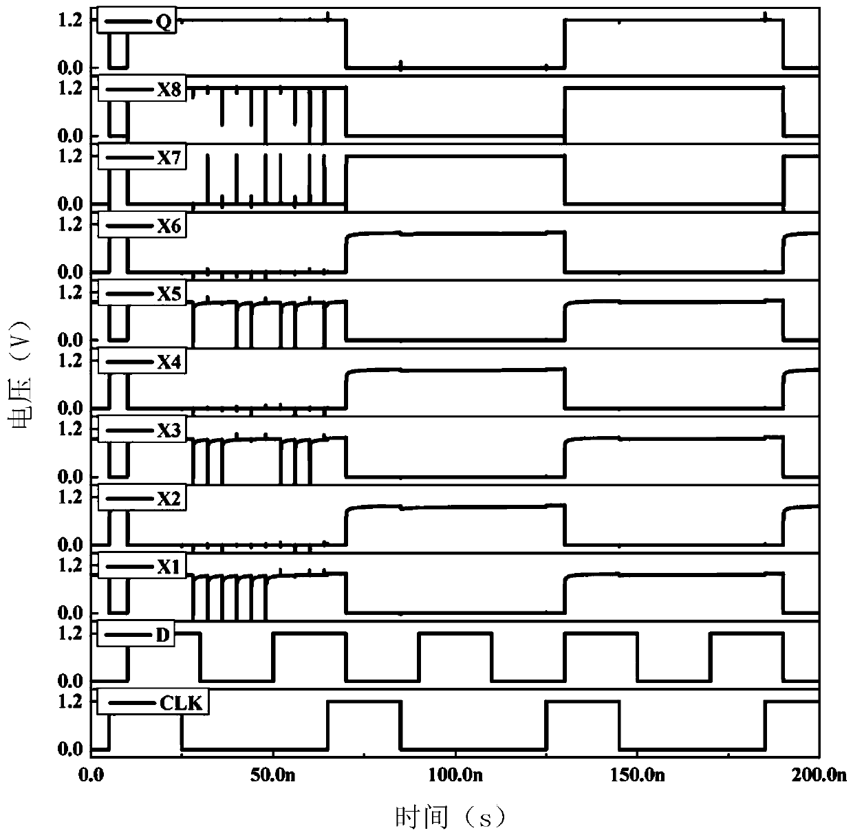
[0061] see figure 1 Describe this embodiment mode. The three-node fault-tolerant stacked D latch for low-p...


PUM


Abstract

The invention discloses a three-node fault-tolerant stack type D latch for low-power-consumption circuit application, which belongs to the field of anti-core reinforcement in integrated circuit reliability. The problems that a traditional D latch resisting three-node overturning needs to consume much hardware, power consumption is high, the area is large, and the number of sensitive nodes is largeare solved. The latch provided by the invention comprises 28 NMOS transistors N1 to N28 and 22 PMOS transistors P1 to P22. According to the invention, the fault tolerance of three nodes is realized by using the polarity of transient pulses generated after the incidence of radiation particles; therefore, the number of sensitive nodes in the circuit is effectively reduced to 5, and the stability ofthe system is improved; meanwhile, the number of used transistors is effectively reduced, and the area and the power consumption overhead of the whole circuit are further reduced; and on the transmission path of the latch, information of an input signal D can be directly transmitted to a node Q through transistors P22 and N28, so that the latch has relatively small propagation delay. The latch provided by the invention is suitable for low and medium frequency circuits.

Description

technical field [0001] The invention belongs to the field of anti-nuclear hardening in integrated circuit reliability. Background technique [0002] Single event upsets mainly occur in memory circuits and sequential logic circuits. When high-energy particles bombard a sensitive node of a memory or a sequential logic circuit, charges accumulate near the sensitive node, causing the level of the other node to jump as well. When the single event reversal effect occurs, high-energy charged particles interact with semiconductor materials, forming a funnel-shaped plasma region along the particle incident path. If there is an electric field in the device at this time, these introduced non-equilibrium carriers will drift and form a transient current, which will cause the potential change of the sensitive node in the circuit to flip. In a circuit with a storage function, due to the preserved structure, the inversion of the value of one node can cause the inversion of another node. ...

Claims


Application Information

Patent Timeline
IPC IPC(8): H03K19/003
CPCH03K19/0013H03K19/00315H03K19/00338
Inventor 朱磊
Owner QIQIHAR UNIVERSITY
Why Eureka
Try Eureka