
OTP memory and manufacturing method thereof

A manufacturing method and memory technology, applied in read-only memory, static memory, semiconductor/solid-state device manufacturing, etc., can solve the problems of large storage unit area, unfavorable application of high density of kilobit level, etc., and improve the writing speed. , read the effect of simple and fast operation

Active Publication Date: 2020-05-08
HUA HONG SEMICON WUXI LTD
View PDF13 Cites 0 Cited by
  • Summary
  • Abstract
  • Description
  • Claims
  • Application Information

AI Technical Summary

Problems solved by technology

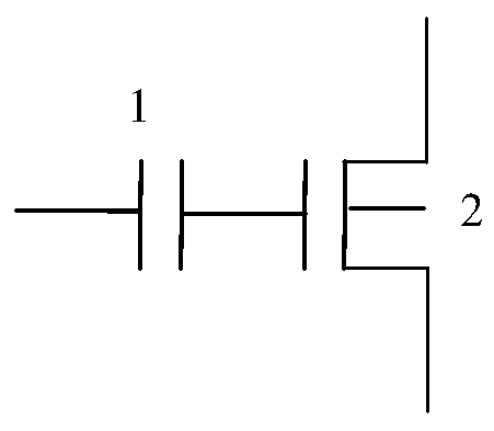
Due to the existence of the floating gate coupling capacitance in the existing first OTP memory, the storage unit area is too large, which is not conducive to the high-density application of the thousand-bit level

Method used


Image

  • OTP memory and manufacturing method thereof
  • OTP memory and manufacturing method thereof
  • OTP memory and manufacturing method thereof

Examples


Embodiment Construction

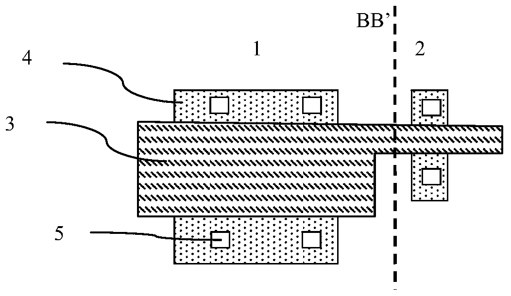
[0068] like Figure 4 Shown, is the layout of the OTP memory of the embodiment of the present invention; As Figure 5 As shown, it is the OTP memory edge of the embodiment of the present invention Figure 4 A cross-sectional view of line AA; the cell structure of the OTP memory according to the embodiment of the present invention includes: a first active region 201 and a second active region 202 .

[0069] The first active region 201 and the second active region 202 vertically intersect each other.

[0070] EDNMOS is formed in the first active region 201 , and PMOS is formed in the second active region 202 .

[0071] The EDNMOS includes a first source region 205, a first channel region 206, a drift region 207, a first drain region 209 and a first gate structure, and the first gate structure is composed of a first gate dielectric layer 214a and a first Polysilicon gates 203 are superimposed, the direction between the first source region 205 and the first drain region 209 is ...


PUM


Abstract

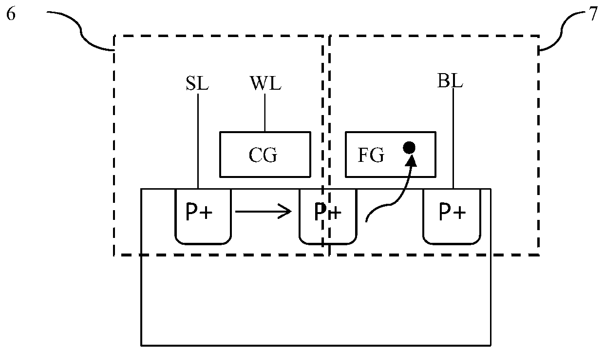
The invention discloses an OTP memory. A unit structure comprises a first active region and a second active region which are vertically intersected, an EDNMOS is formed in the first active region, anda PMOS is formed in the second active region; a main body part of a channel region of the PMOS is composed of a drift region of an EDNMOS, a first polysilicon gate of the EDNMOS serves as a control gate, and a second polysilicon gate of the PMOS serves as a floating gate; and programming of the PMOS is performed by utilizing hot carriers formed in the drift region of the EDNMOS. The invention further discloses a manufacturing method of the OTP memory. High-speed writing can be realized.

Description

technical field [0001] The invention relates to the field of semiconductor integrated circuit manufacturing, in particular to a one-time programmable (one-time programmable memory, OTP) memory; the invention also relates to a method for manufacturing the OTP memory. Background technique [0002] OTP memory is a common non-volatile memory (NVM), which has more applications in embedded NVM with limited density and limited performance. Traditional electrically erasable programmable read-only memory (EEPROM), S0NOS, embedded flash memory (E-Flash) NVM is expensive. OTP memory and CMOS-compatible embedded NVM technology is a successful solution in the current industry, and it has been widely used in applications such as analog technology trimming from the bit level to the kilobit level of data or code storage. . [0003] There are many types of structural designs of OTP memory cells. There are three main types of representative ones: [0004] The first type is the capacitive ...

Claims


Application Information

Patent Timeline
Patent Type & Authority Applications(China)
IPC IPC(8): H01L27/112
CPCH10B20/30H10B20/25H01L29/7885H01L29/42324H01L21/26513G11C17/08G11C16/0433
Inventor 刘俊文陈华伦
Owner HUA HONG SEMICON WUXI LTD
Learn More