Chip stacking packaging body with electromagnetic shielding function and preparation method thereof
A chip stacking and electromagnetic shielding technology, applied in the direction of electric solid devices, circuits, electrical components, etc., can solve the problems of unable to guarantee microwave/millimeter wave bare chips, unable to meet the packaging requirements of microwave/millimeter wave bare chips, etc., and achieve circuit layout Reduced space, improved integration, and small size
- Summary
- Abstract
- Description
- Claims
- Application Information
AI Technical Summary
Problems solved by technology
Method used
Image

Examples
Embodiment 2
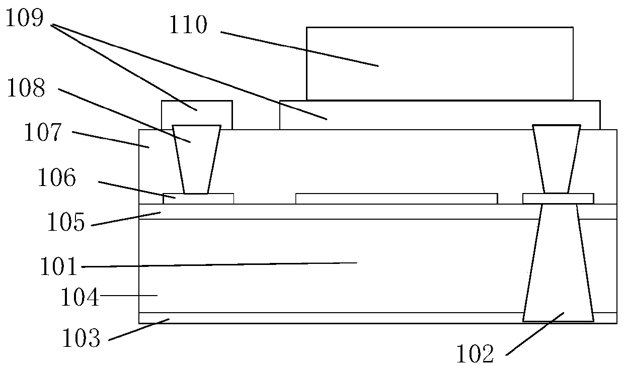
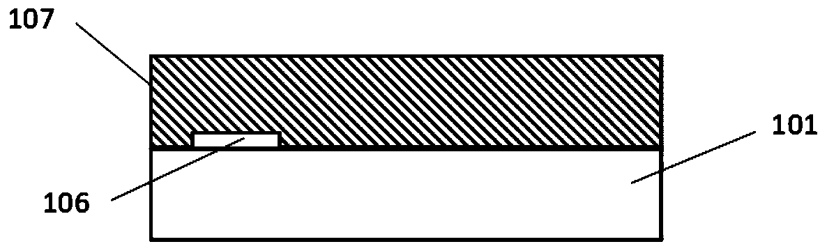
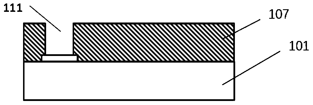
[0051] Another specific embodiment of the present invention discloses a method for preparing a chip stack package with electromagnetic shielding function in Embodiment 1, which specifically includes the following steps:
[0052] Step 1: setting a packaging dielectric layer 107 on the surface of the microwave / millimeter wave bare chip 101 to be packaged.
[0053] The surface of the microwave / millimeter wave bare chip 101 to be packaged is cleaned, and a layer of packaging medium layer 107 is coated on the surface of the microwave / millimeter wave bare chip 101 with a glue spreader, such as figure 2 shown. The material of the packaging dielectric layer 107 is polyimide, and the thickness of the packaging dielectric layer 107 is 8-10um, preferably 9um. This thickness parameter setting overcomes the performance of the microwave / millimeter wave bare chip 101 when the thickness of the packaging dielectric layer 107 is too thin. Defects that cause deterioration, excessive thickness ...
PUM
 Abstract
Description
Claims
Application Information
 - R&D
- Intellectual Property
- Life Sciences
- Materials
- Tech Scout
- Unparalleled Data Quality
- Higher Quality Content
- 60% Fewer Hallucinations
Browse by: Latest US Patents, China's latest patents, Technical Efficacy Thesaurus, Application Domain, Technology Topic, Popular Technical Reports.
© 2025 PatSnap. All rights reserved.Legal|Privacy policy|Modern Slavery Act Transparency Statement|Sitemap|About US| Contact US: help@patsnap.com