Method for depositing an insulating material into a via

A technology of insulating material layer and conductive hole, applied in metal material coating process, circuit, electrical components and other directions, can solve the problem of unavailability and so on

Active Publication Date: 2020-04-17
COOPERS GMBH
View PDF7 Cites 0 Cited by
  • Summary
  • Abstract
  • Description
  • Claims
  • Application Information

AI Technical Summary

Problems solved by technology

[0014] The deposition technique of the present invention cannot achieve a "discontinuity" in the thickness at the bottom of the via, thus requiring extensive etching in subsequent steps to make contact with the metal present below the via

Method used


Image

  • Method for depositing an insulating material into a via
  • Method for depositing an insulating material into a via
  • Method for depositing an insulating material into a via

Examples


Embodiment approach

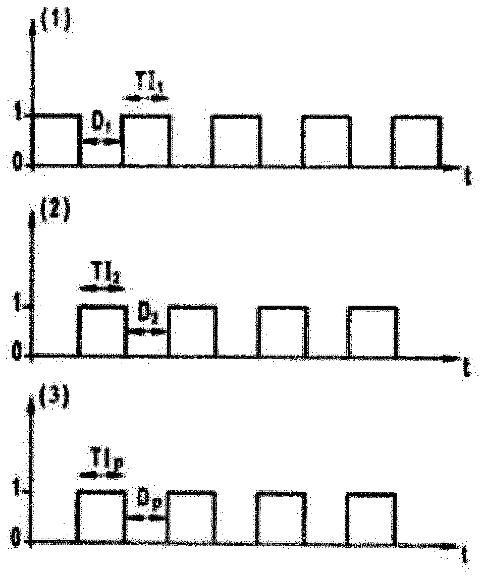
[0071] - the duration TI1 of one pulse of the first pulse sequence and / or the duration TI2 of one pulse of the second pulse sequence may be in the range of 0.02 s to 1 s, respectively;

[0072] - the time interval D1 between two pulses of the first pulse sequence and the time interval D2 between two pulses of the second pulse sequence may be in the range of 0.02s to 1s, respectively;

[0073] According to other implementations:

[0074] - the duration TI1 of one pulse of the first pulse sequence and the duration TI2 of one pulse of the second pulse sequence may be in the range of 1 s to 5 s, respectively;

[0075] - the time interval D1 between two pulses of the first pulse sequence and the time interval D2 between two pulses of the second pulse sequence may be in the range of 1 s to 10 s, respectively;

[0076] By definition, a plasma corresponds to an excited or ionized state of a gas, which further corresponds to the transfer of electrical energy from an electrical source ...

no. 1 approach

[0087] Similar to Sequence 1 and Sequence 2, the following terms are defined for Sequence 3 of the plasma as follows:

[0088] - Duration of one plasma pulse: TIp

[0089] - Time interval between two consecutive plasma pulses: Dp.

[0090] In the specific example of plasma sequence 3, the plasma pulse corresponds to the pulse of injection sequence 2 of the second chemical species. Thus, duration TIp corresponds to duration TI2, and time interval Dp corresponds to time interval D2.

[0091] E.g,

[0092] - the duration TIp of one plasma pulse may be in the range of 0.02s to 5s, and the time interval Dp between two plasma pulses may be in the range of 0.02s to 10s;

[0093] - the duration TIp of one plasma pulse may be in the range of 0.02s to 1s, and the time interval Dp between two plasma pulses may be in the range of 0.02s to 1s;

[0094] - the duration TIp of one plasma pulse may be in the range of 1 s to 5 s, and the time interval Dp between two plasma pulses may be in ...


PUM


Abstract

A method for depositing a layer (4, 5, 6) of a material onto a substrate (20), comprising: -one gas-phase injection of a first chemical species with a precursor of such insulating material, into a deposition chamber of a chemical vapor deposition reactor, through a first injection path, according to a first pulse sequence; -one gas-phase injection of a second chemical species with a reactant adapted to react with such precursor, into the deposition chamber, through a second injection path, according to a second pulse sequence which is phase-shifted relative to the first pulse sequence; -one sequential generation of a plasma of the first chemical species and / or the second chemical species during at least one pulse of at least one of the first and second sequences, with such plasma being generated from a high frequency (HF) plasma source and a low frequency (LF) plasma source applied to the first and second injection paths, the low frequency (LF) plasma source power on the high frequency(HF) plasma source power ratio being above 1.

Description

technical field [0001] The present invention relates to a method of depositing insulating (ie dielectric) material into conductive vias (vias), more precisely "through silicon vias". [0002] Such a deposition method is a special implementation of a method for spraying chemical species in a gaseous state, for applications such as vapor deposition of a layer onto a substrate in a reactor. Background technique [0003] Various manufacturing or surface treatment methods include the steps of sequentially injecting gaseous reactants into a reactor. This results in the reactants being injected in a pulsed sequence, as opposed to continuously injecting the reactants into the reactor. Such pulsed injection allows better control over the amount of reactive elements introduced, the duration of contact between the various reactants and their residence time in the reactor. [0004] Among the methods using pulsed injection of reactants, mention may be made of "chemical vapor deposition...

Claims


Application Information

Patent Timeline
Patent Type & Authority Applications(China)
IPC IPC(8): C23C16/04C23C16/455C23C16/505H01L21/02
CPCC23C16/045C23C16/45523C23C16/45574C23C16/505H01L21/0228H01L21/02164H01L21/0217H01L21/02178H01L21/02216H01L21/02219H01L21/02274H01L21/76898H01L21/76877C23C16/45553
Inventor 法比安·皮亚拉朱利安·维蒂耶洛
Owner COOPERS GMBH
Why Eureka
Try Eureka