High-speed laser processing device and method based on spatial light modulator and scanning galvanometer
A spatial light modulator and laser processing technology, applied in manufacturing tools, laser welding equipment, metal processing equipment, etc., can solve problems such as processing efficiency limitations, and achieve the effects of small energy loss, wide range of laser light sources, and good flexibility
- Summary
- Abstract
- Description
- Claims
- Application Information
AI Technical Summary
Problems solved by technology
Method used
Image
Examples
Embodiment 1
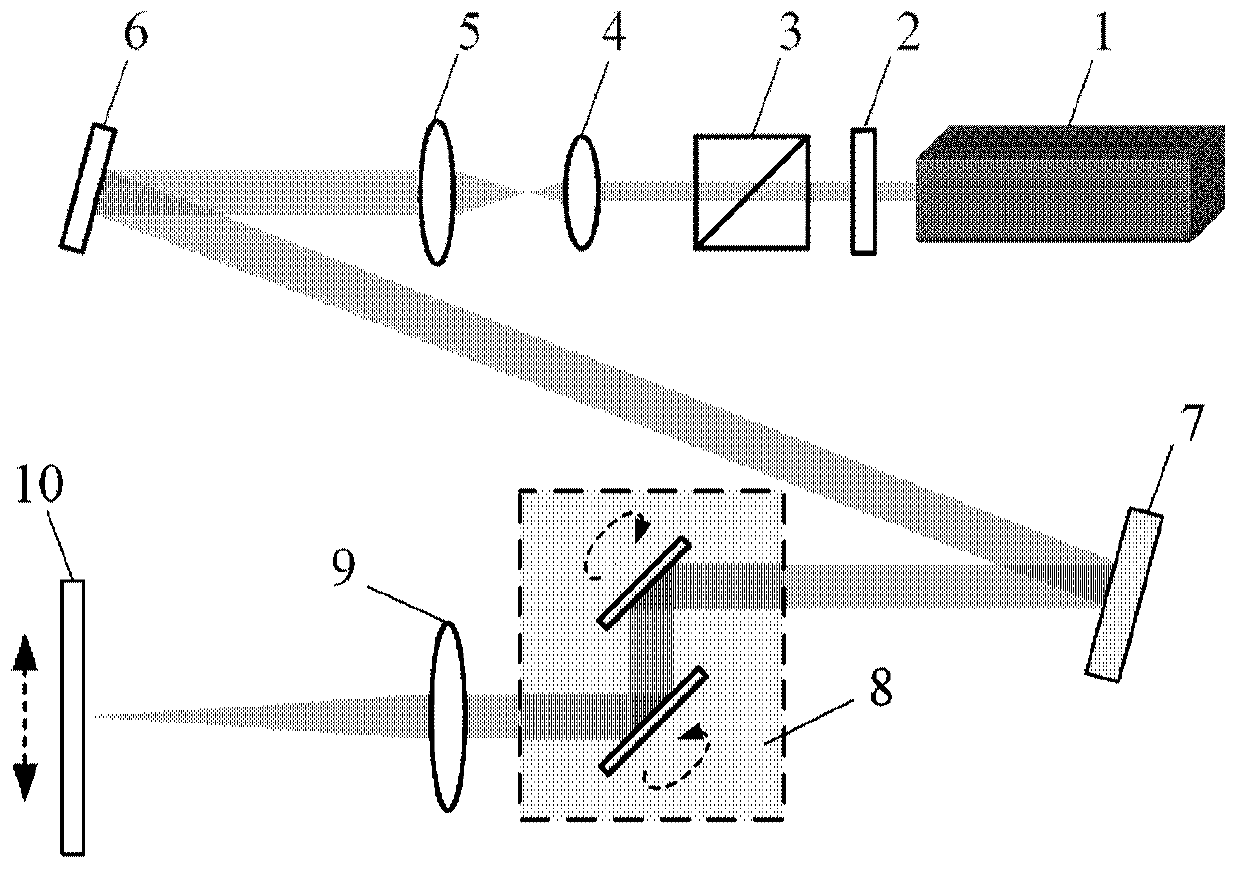
[0061] For the application scenarios of large-scale high-efficiency laser marking or surface treatment, the optical path system such as figure 1 shown. Among them, the λ / 2 wave plate 2 and the polarizing prism 3 form a beam energy attenuator, which is used to control the energy and polarization state of the beam; the first lens 4 and the second lens 5 expand the beam; the spatial light modulator 7 passes Load the pre-designed computational hologram to realize the adjustment of the phase distribution of the incident beam (for the application of high-power laser, the spatial light modulation device can be replaced with a customized phase plate or grating), and the phase-adjusted beam enters the galvanometer system, The deflection following the galvanometer angle achieves 2θ deflection. The deflected beam enters the flat-field lens for focusing, and its focal point will perform high-speed translation in the two-dimensional space of the focal plane to realize the processing of ma...
Embodiment 2
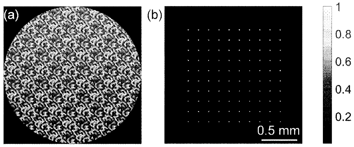
[0064] For the application scenarios of large-scale high-efficiency laser marking or surface treatment, the scanning speed can be increased by more than an order of magnitude (greater than 500m / s) by using a high-resonance frequency scanning galvanometer (12kHz). Combined with parallel scanning of 10×10 multi-focus array, the processing speed of traditional laser marking can be further increased by two orders of magnitude; with the z-phase linear moving platform, scanning and switching of different layers can be realized, so that the system can be used to complete laser three-dimensional forming or three-dimensional Print;
Embodiment 3
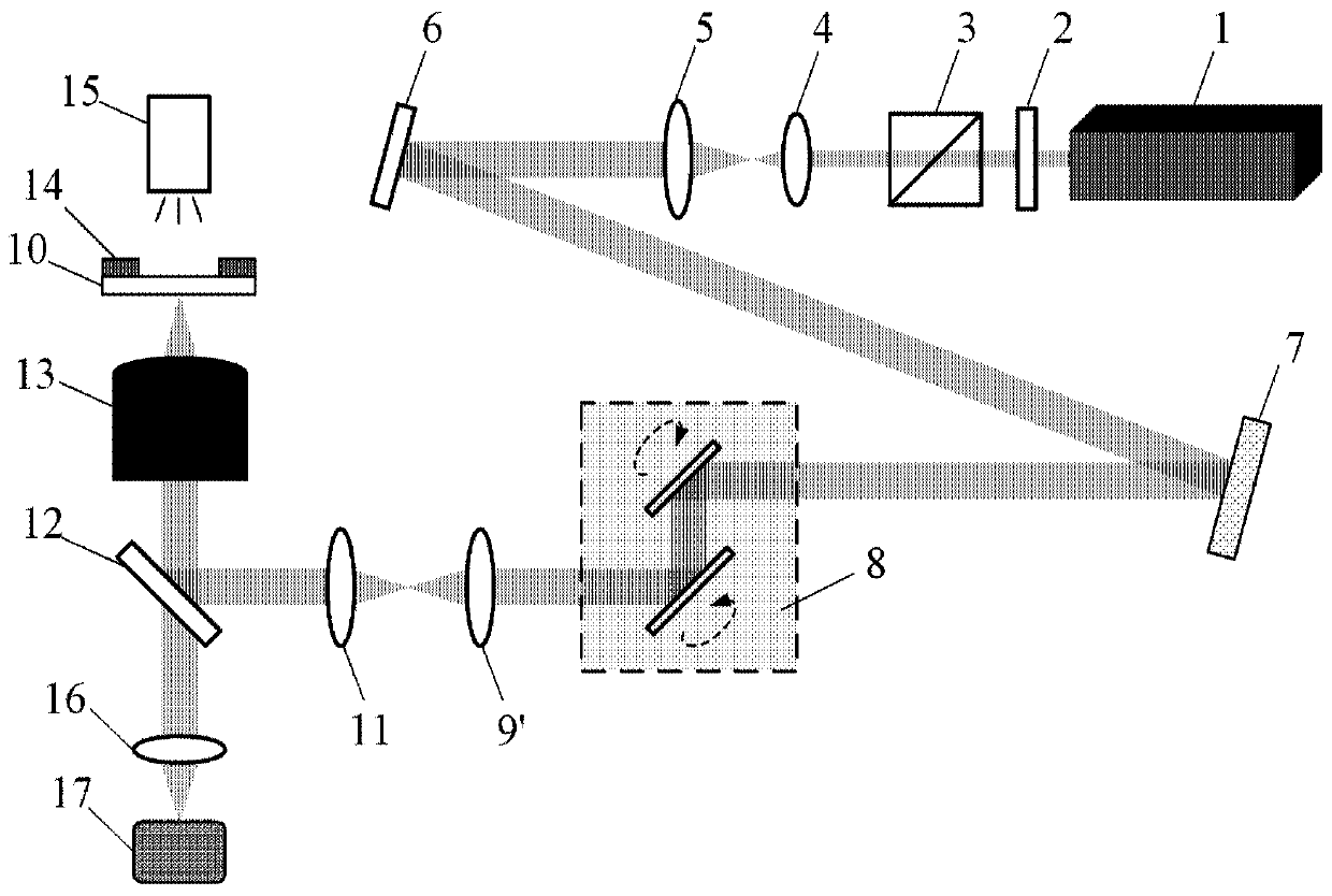
[0066] For the application scenario of laser micro-nano processing, the optical system such as figure 2 shown. At this time, it is necessary to add a 4f optical system after the scanning galvanometer system, and replace the focusing lens with a high numerical aperture objective lens. And increase the corresponding real-time observation module. The phase-adjusted beam enters the galvanometer system, and follows the angular deflection of the galvanometer for 2θ deflection. The deflected light beam enters the 4f system (the third lens 9', the fourth lens 11), which is used to control the deflection displacement of the light beam before entering the focusing lens. The laser beam then enters the 12-microscope objective lens to achieve focused processing of the material. The multi-focus array realizes the parallel scanning of the single-layer plane through the deflection of the scanning galvanometer, and uses the linear nano-piezoelectric positioning platform to realize the z-ax...
PUM
 Abstract
Description
Claims
Application Information
 - R&D
- Intellectual Property
- Life Sciences
- Materials
- Tech Scout
- Unparalleled Data Quality
- Higher Quality Content
- 60% Fewer Hallucinations
Browse by: Latest US Patents, China's latest patents, Technical Efficacy Thesaurus, Application Domain, Technology Topic, Popular Technical Reports.
© 2025 PatSnap. All rights reserved.Legal|Privacy policy|Modern Slavery Act Transparency Statement|Sitemap|About US| Contact US: help@patsnap.com


