Display device manufacturing method and display device
A display device and manufacturing method technology, applied in semiconductor/solid-state device manufacturing, semiconductor devices, electric solid-state devices, etc., can solve problems such as process difficulty, and achieve the effects of cost reduction, small bending R angle, and small frame
- Summary
- Abstract
- Description
- Claims
- Application Information
AI Technical Summary
Problems solved by technology
Method used
Image
Examples
Embodiment 1
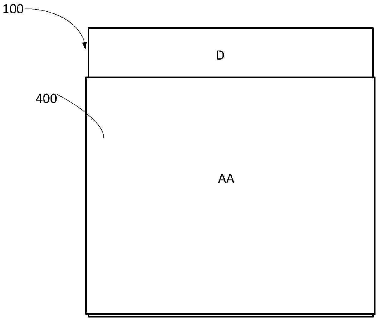
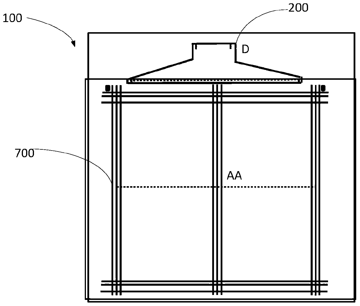
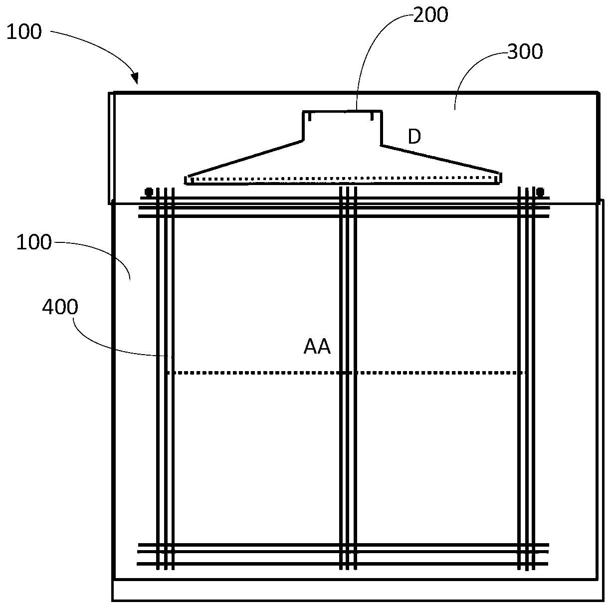
[0106] Figure 1-7 It is a schematic flowchart of the manufacturing method of the display device provided in Example 1.
[0107] Figure 8-10 , Figure 19 Shown are several exemplary structural schematic diagrams of the display device obtained by step S11 in this embodiment.
[0108] In Embodiment 1 provided by the present invention, before the peripheral circuit 200 is formed on the first surface of the base substrate 100 at the bonding area D, that is, before step S2, a Buffer peeling layer 400, the function of this buffer peeling layer 400 is to increase the adhesion between the metal layer and the base substrate 100, so that when the binding region D on the base substrate 100 is removed (for example, by laser cutting or mechanical cutting and other processes to cut the base substrate 100), the peripheral circuit 200 is peeled from the base substrate 100 to the flexible insulating film 300, due to the setting of the buffer peeling layer 400, the metal layer in the display...
Embodiment approach
[0121] The first implementation mode:
[0122] Described step 2 specifically comprises:
[0123] Step A, forming a first-layer metal layer 10 on the first surface of the base substrate 100, the first-layer metal layer 10 including the peripheral circuit 200 located in the bonding area D;
[0124] Step B, covering the first metal layer 10 with a flexible insulating film 300, and covering the thin film transistor drive array 700 in the display area AA with an insulating layer, wherein the insulating layer partially covers the peripheral circuit, and on the forming via holes on the insulating layer at positions corresponding to the peripheral circuits;
[0125]Step C, forming a thin film transistor driving array 700 located in the display area AA on the flexible insulating film 300 and the insulating layer, the thin film transistor driving array 700 includes signal wiring including gate lines, data lines and TFTs, and the TFT driving array 700 is electrically connected to the f...
Embodiment 2
[0160] Figure 26 with 27 Shown is a second exemplary structural schematic diagram of the display device obtained by step S11.
[0161] Such as Figure 26 with 27 As shown, in the second embodiment provided by the present invention, before the peripheral circuit 200 is formed on the first surface of the base substrate 100 at the bonding region D, that is, before step S2, the substrate A release layer 500 is formed at the bonding region D of the substrate 100 , and the function of the release layer 500 is to reduce the adhesion between the metal layer and the base substrate 100 .
[0162] In this way, when the base substrate 100 is partially cut by means of mechanical cutting or laser cutting to remove the binding region D of the base substrate 100, due to the setting of the peeling layer 500 in the binding region D, the metal layer ( The adhesive force between the peripheral circuit 200 ) and the base substrate 100 makes the bonding area D of the base substrate 100 and the...
PUM
| Property | Measurement | Unit |
|---|---|---|
| thickness | aaaaa | aaaaa |
Abstract
Description
Claims
Application Information
 - R&D
- Intellectual Property
- Life Sciences
- Materials
- Tech Scout
- Unparalleled Data Quality
- Higher Quality Content
- 60% Fewer Hallucinations
Browse by: Latest US Patents, China's latest patents, Technical Efficacy Thesaurus, Application Domain, Technology Topic, Popular Technical Reports.
© 2025 PatSnap. All rights reserved.Legal|Privacy policy|Modern Slavery Act Transparency Statement|Sitemap|About US| Contact US: help@patsnap.com


