Method for improving sensitivity of gas sensor
A gas sensor and sensitivity technology, used in instruments, scientific instruments, measuring devices, etc., can solve the problems of low sensitivity and poor effect, and achieve the effect of good sensitivity and improved sensitivity
- Summary
- Abstract
- Description
- Claims
- Application Information
AI Technical Summary
Problems solved by technology
Method used
Image
Examples
Embodiment 1
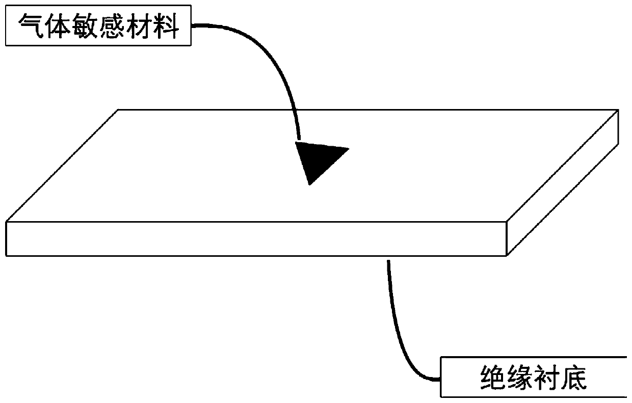
[0035] A method for improving the sensitivity of a gas sensor requires only replacing the metal of an electrode connected to a gas-sensitive material with manganese metal. The gas sensitive material is SnS 2 ;
[0036] as attached figure 1 As shown in , in operation step 1, a piece of gas-sensitive material is transferred to an insulating substrate, for example, SnS 2 Material is transferred to glass slides.
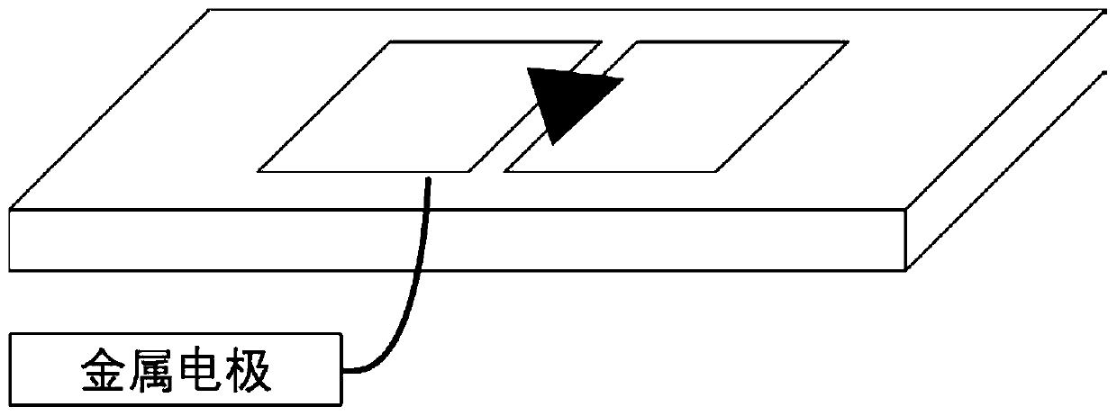
[0037] as attached figure 2 As shown in , the operation step 2 is to make a mask on the gas-sensitive material. First, a suitable mask is formed by ultraviolet photolithography, and then a layer of manganese metal is plated on one side of the mask by vacuum evaporation. , and then wash off the mask with acetone alcohol to form the required conductive electrodes. For ease of illustration, only the 2-terminal electrode is shown in the figure, and more complex electrode structures can also be used.
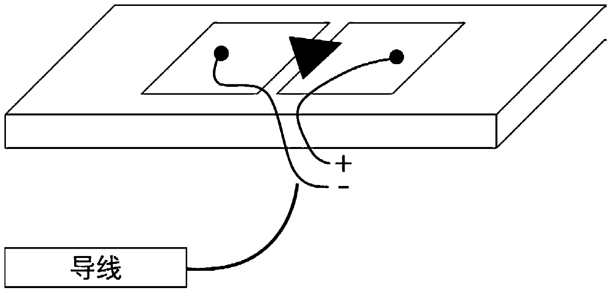
[0038] as attached image 3 As shown in , in operation step 3, the...
Embodiment 2
[0043] as attached Figure 8 As shown in , this is a schematic diagram showing the effect of the built-in electric field formed at the metal-semiconductor contact interface on the gas sensor.
[0044] This figure uses manganese metal (4.1eV) as the electrode contacting SnS 2 (5.36eV) gas sensitive material, the target molecule absorbed is NO 2 .
[0045] Figure 8 In, the solid line is the adsorption of NO 2 The current-voltage relationship before the gas, the vertical dotted line is the bias voltage V applied at both ends of the sensor during detection 0 , the horizontal dotted line is the corresponding current I at this moment 0 ; When the sensor adsorbs NO 2 After the gas molecules, part of the charge accumulated at the metal-semiconductor contact interface is bound, which is equivalent to reducing the SnS at the interface. 2 The Fermi surface, and the metal-semiconductor contact in order to achieve the Fermi surface balance, the electrons in the metal will continue ...
PUM
 Abstract
Description
Claims
Application Information
 - Generate Ideas
- Intellectual Property
- Life Sciences
- Materials
- Tech Scout
- Unparalleled Data Quality
- Higher Quality Content
- 60% Fewer Hallucinations
Browse by: Latest US Patents, China's latest patents, Technical Efficacy Thesaurus, Application Domain, Technology Topic, Popular Technical Reports.
© 2025 PatSnap. All rights reserved.Legal|Privacy policy|Modern Slavery Act Transparency Statement|Sitemap|About US| Contact US: help@patsnap.com


