
Power semiconductor module

A power semiconductor and molding technology, applied in the direction of semiconductor devices, semiconductor/solid-state device manufacturing, semiconductor/solid-state device components, etc., to achieve the effect of improving long-term reliability

Pending Publication Date: 2020-03-24
HITACHI ENERGY SWITZERLAND AG
View PDF16 Cites 0 Cited by
  • Summary
  • Abstract
  • Description
  • Claims
  • Application Information

AI Technical Summary

Problems solved by technology

[0017] However, there is still room for improvement in the solutions of the prior art, for example with regard to providing effective measures against negative influences on power semiconductor devices and thus with regard to long-life reliability

Method used


Image

  • Power semiconductor module
  • Power semiconductor module
  • Power semiconductor module

Examples


Embodiment Construction

[0075] Reference will now be made in detail to the exemplary embodiments illustrated in the drawings. This example is provided by way of explanation and is not intended to be limiting. It is intended that the present disclosure includes such modifications and variations.

[0076] Within the following description of the drawings, the same reference numbers refer to the same components. In general, only the differences with respect to individual embodiments are described. When several identical items or parts appear in a drawing, not all parts have a reference number in order to simplify the layout.

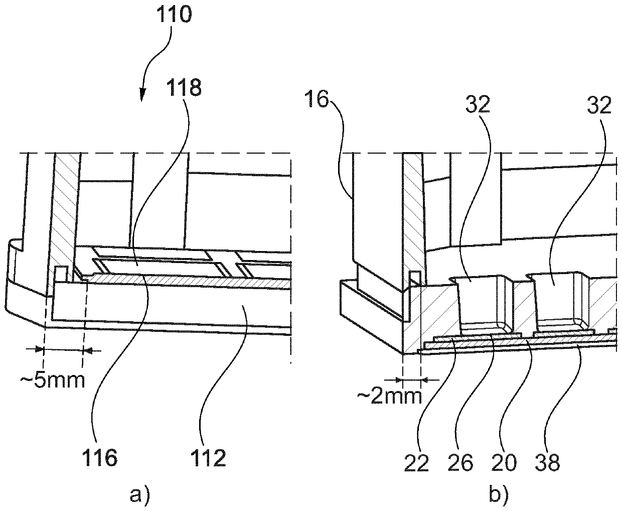
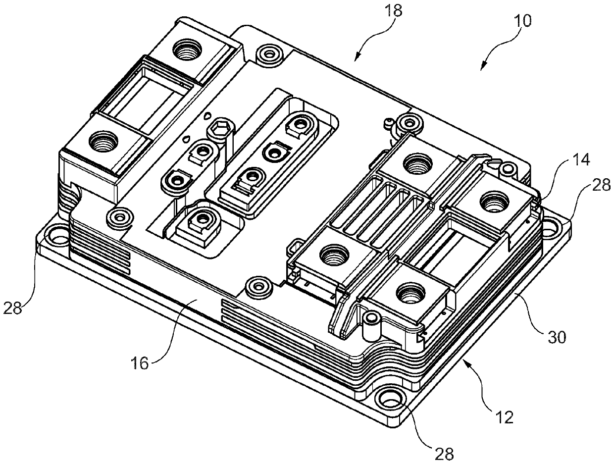
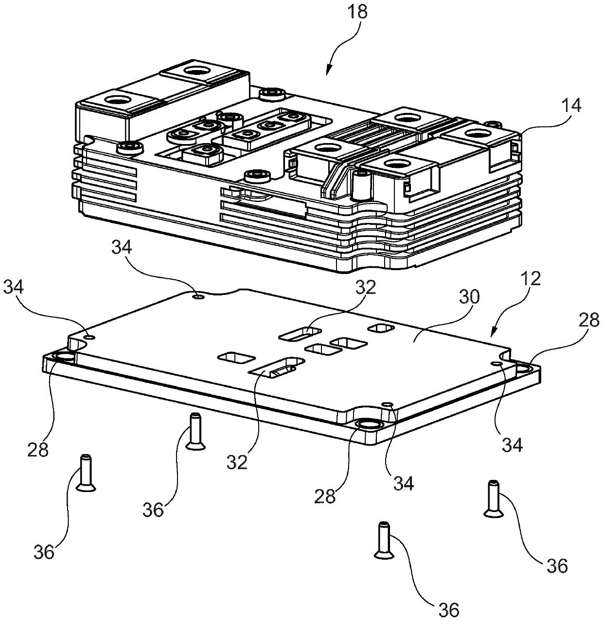
[0077] figure 1 A power semiconductor module 10 is shown. The power semiconductor module 10 includes a substrate 12 and a housing 14 . exist figure 2 and image 3 In , the substrate 12 is shown in more detail. As described in more detail below, the housing 14 includes a circumferential side wall 16 . Furthermore, the housing includes its active peripherals 18 including, ...


PUM


Abstract

The present invention provides a power semiconductor module (10), comprising a substrate (12) having an electric insulating main layer (20) being provided with a structured top metallization (22) andwith a bottom metallization (38), wherein the top metallization (22) is provided with at least one power semiconductor device (24) and at least one contact area (26), wherein the main layer (20) together with its top metallization (22) and the at least one power semiconductor device (24) is embedded in a mold compound (30) such that the mold compound (30) comprises at least one opening (32) for contacting the at least one contact area (26), and wherein power semiconductor module (10) comprises a housing (14) with circumferential side walls (16), wherein the side walls (16) are positioned abovethe main layer (20) of the substrate (12) so that the side walls (16) are only present in a space above a plane through the main layer (20) of the substrate (12).

Description

technical field [0001] The invention relates to power semiconductor modules. The invention relates in particular to power semiconductor modules which exhibit good long-life reliability, good performance and can be produced at low cost. Background technique [0002] Power semiconductor modules comprising power semiconductor devices, such as switching power semiconductor devices, are generally known in the art. For a particular application, it may be important to protect the power semiconductor device mechanically and / or with respect to environmental factors, in order for the module to work reliably for a long time. [0003] US 2010 / 0133684 A1 describes a power semiconductor module comprising: a circuit board with a metal base plate, a highly thermally conductive insulating layer, and a wiring pattern; a power semiconductor element, which is electrically connected to the wiring pattern; a tubular external terminal connection body, which provided for wiring patterns, for exte...

Claims


Application Information

Patent Timeline
IPC IPC(8): H01L23/049H01L23/31H01L23/40H01L25/07
CPCH01L23/4006H01L25/072H01L23/053H01L21/481H01L21/565H01L23/08H01L23/142H01L23/29H01L23/3178
Inventor D.特吕泽尔S.哈特曼D.吉永
Owner HITACHI ENERGY SWITZERLAND AG
Learn More