Method and substrate for improving warpage of asymmetric copper thick substrate

A thick substrate, asymmetric technology, used in the structural connection of printed circuits, electrical components, printed circuit components, etc., can solve problems such as warpage, reduce stress differences, and ensure product quality.

Active Publication Date: 2021-06-18
广州陶积电电子科技有限公司
View PDF10 Cites 0 Cited by
  • Summary
  • Abstract
  • Description
  • Claims
  • Application Information

AI Technical Summary

Problems solved by technology

[0003] In view of the problem of warping in the processing of the existing asymmetric copper thick substrate, the present invention proposes a method for improving the warpage of the asymmetric copper thick substrate. The specific scheme is as follows:

Method used


Image

  • Method and substrate for improving warpage of asymmetric copper thick substrate
  • Method and substrate for improving warpage of asymmetric copper thick substrate
  • Method and substrate for improving warpage of asymmetric copper thick substrate

Examples


Embodiment Construction

[0027] In order to fully understand the technical content of the present invention, the technical solution of the present invention will be further introduced and illustrated below in conjunction with specific embodiments.

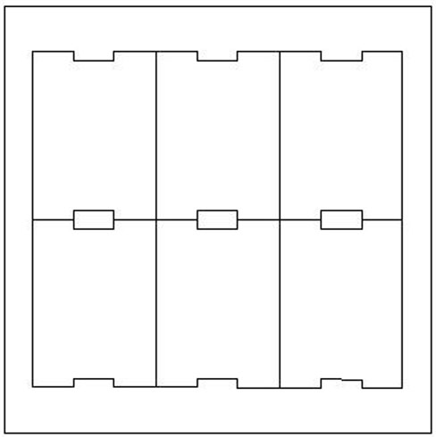
[0028] Step 1: jigsaw puzzle is the basic method to improve production efficiency, such as figure 1 As shown, put 6 pieces of the same product picture together in the fixed frame, center them, and adjust the distance between the whole product picture and each side of the fixed frame to keep it at about 8mm.

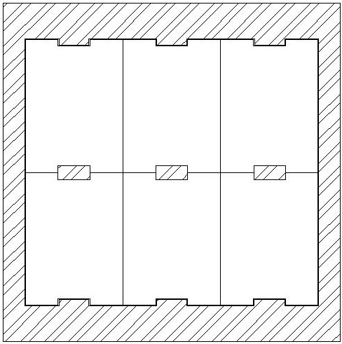
[0029] Step 2: Lay copper on the frame, such as figure 2 As shown, on the process edge other than the product drawing, there are copper graphics. In order to ensure a certain processing distance between the product and the process edge for subsequent cutting processing, along the inner edge of the process edge, the frame Part of the copper is cut off, so that the distance between the process edge and the product drawing is about 0.5mm.
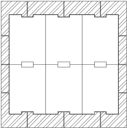
[0030] Ste...


PUM


Abstract

The invention discloses a method and a substrate for improving the warpage of an asymmetric copper thick substrate, comprising the steps of: performing process edge division on a thicker copper layer when performing CAM processing on a substrate with asymmetric copper thickness at both ends of an insulating layer If the substrate is still warped, then increase or decrease the graphics at both ends according to the difference in copper thickness and quality at both ends. In the present invention, during the CAM process, the end of the copper thickness is divided into small pieces, which reduces the stress difference between the layers, thereby improving the warpage of the substrate. Deleting graphics on the process side of the larger mass, or adding graphics to the process side of the smaller mass end, so as to improve the stress difference on both sides of the substrate and reduce the warpage.

Description

technical field [0001] The invention belongs to the technical field of substrate production, in particular to a method for improving the warping of an asymmetric copper thick substrate and a substrate. Background technique [0002] With the continuous development of electronic technology, more and more functional circuits are concentrated in the PCB board. The substrate is the production basis of the PCB board, and its processing is particularly important. The copper thickness between the substrate layers is asymmetrical, usually in the middle On the two sides of the insulating layer, the distribution of copper thickness is inconsistent, also known as copper thickness asymmetry or asymmetry. Inconsistent copper thickness usually means that the copper thickness differs by more than 18 microns. The substrate with asymmetrical copper thickness, with the intermediate insulating layer as the two sides of the symmetric plane, after processing, the stress is inconsistent, and warp...

Claims


Application Information

Patent Timeline
Patent Type & Authority Patents(China)
IPC IPC(8): H05K3/00H05K1/14
CPCH05K1/142H05K3/0044H05K3/0097
Inventor 徐朝晨徐上廷钟鸿枫钟少瑛
Owner 广州陶积电电子科技有限公司
Why Eureka
Try Eureka