Packaging structure for system heat dissipation and packaging process

A technology of packaging structure and packaging process, applied in the direction of semiconductor/solid-state device components, semiconductor devices, electrical components, etc., can solve the problems of too large heat flow density and too small heat dissipation path of packaging chips that cannot be improved, and achieve improved heat transfer performance. , Improve heat dissipation performance, good heat dissipation effect

Pending Publication Date: 2020-02-18
SHANGHAI XIANFANG SEMICON CO LTD +1
View PDF0 Cites 1 Cited by
  • Summary
  • Abstract
  • Description
  • Claims
  • Application Information

AI Technical Summary

Problems solved by technology

[0004] The technical problem to be solved by the present invention is that the existing traditional heat dissipation methods cannot improve the problems of excessive heat flux density and small heat dissipation paths inside the packaged chip; the present invention provides a package for system heat dissipation that solves the above problems Structure and packaging process

Method used


Image

  • Packaging structure for system heat dissipation and packaging process
  • Packaging structure for system heat dissipation and packaging process

Examples


Embodiment 1

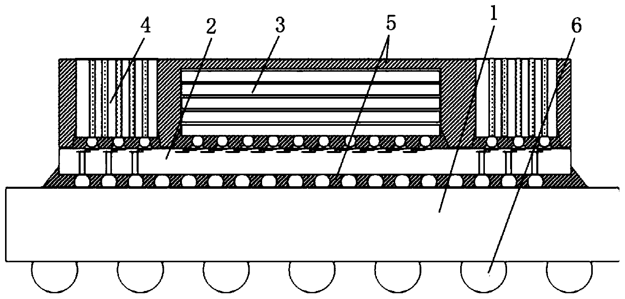
[0042] A package structure for system heat dissipation, such asfigure 1 As shown, it includes: a substrate 1, an active chip 2, a memory chip 3, a heat conductor 4 and a package body 5; wherein, the active chip 2 is mounted on the substrate 1; the memory chip 3 is mounted on the active chip 2; The heat conductor 4 and the memory chip 3 are mounted on the same surface of the active chip 2, and the heat conductor 4 has a second TSV interconnected with the active chip 2; the package body 5 integrates the active chip 2, The memory chip 3 and the heat conductor 4 are packaged on the substrate 1 , one end of the second TSV on the heat conductor 4 is interconnected with the active chip 2 , and the other end of the second TSV is exposed on the surface of the package 5 .

[0043] Through the setting of the above structure, the heat on the memory chip 3 can be introduced to the active chip 2, and then a large amount of heat on the active chip 2 can be exported to the air through the seco...

Embodiment 2

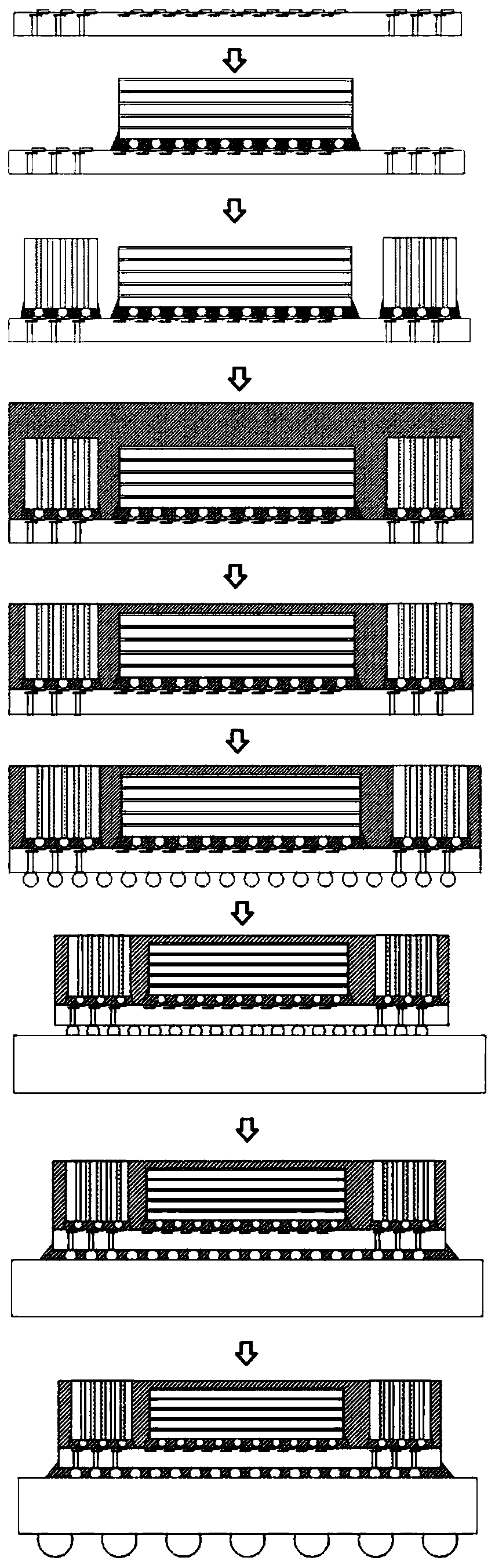
[0049] This embodiment provides a packaging process for a packaging structure for system heat dissipation, such as figure 2 As shown, the specific process is as follows:

[0050] Step 1: Mount the memory chip 3 and the heat conductor 4 with the second TSV on the same side of the active chip 2 . In the present invention, the memory chip 3 is mounted on the active chip 2 first, and then the heat conductor 4 is mounted on the active chip 2 . The memory chip 3 can be mounted on the front of the active chip 2, and can also be mounted on the back of the active chip 2; when mounted on the back, the interconnection between the active chip 2 and the memory chip 3 can be realized through leads; When it is on the front side, the back side of the memory chip 3 can be used to mount on the front side of the active chip 2. At this time, the interconnection between the memory chip 3 and the active chip 2 can be realized through leads, or the front side of the memory chip 3 can be used to be...


PUM


Abstract

The invention discloses a packaging structure for system heat dissipation and a packaging process. The packaging structure in the present invention includes: a substrate; an active chip mounted on thesubstrate; a memory chip mounted on the active chip; a thermal conductor, wherein the thermal conductor and the memory chip are mounted on the same side of the active chip, and a second TSV interconnected with the active chip is disposed on the thermal conductor; and a packaging body packaging the active chip, the memory chip and the thermal conductor on the substrate, wherein one end of the second TSV on the thermal conductor is interconnected with the active chip, and the other end of the second TSV is exposed on the surface of the packaging body. The packaging structure enlarges the heat dissipation path of the packaging structure itself, thereby significantly improving the heat dissipation performance.

Description

technical field [0001] The invention relates to the field of chip packaging, in particular to a packaging structure for system heat dissipation and a packaging process thereof. Background technique [0002] At present, the traditional main path of chip heat dissipation includes two aspects, one is the back of the chip package, and the other is the PCB board. At present, heat dissipation is mainly carried out by adding a heat dissipation cover on the package surface, improving the thermal conductivity of the thermal interface material, adding active heat dissipation structures such as forced cooling, and improving the design of the package substrate. Without adding an active heat dissipation structure, most of the heat is actually exported through the PCB board, which is mainly for some low-power products. In products that require an active heat dissipation structure, the main heat dissipation path has changed to the back of the chip-heat sink-air path. [0003] With the co...

Claims


Application Information

Patent Timeline
Patent Type & Authority Applications(China)
IPC IPC(8): H01L23/367H01L23/31H01L23/48H01L25/18H01L21/98
CPCH01L23/367H01L23/3677H01L23/3107H01L23/481H01L25/18H01L25/50H01L2224/16225H01L2224/73204H01L2224/32225H01L2924/15311H01L2224/32145H01L2924/00
Inventor 孙鹏徐成任玉龙曹立强
Owner SHANGHAI XIANFANG SEMICON CO LTD
Why Eureka
Try Eureka