Surface Wave Suppression Method on Temperature Compensation Layer of Temperature Compensation Surface Acoustic Wave Device
A surface acoustic wave device, temperature compensation technology, applied in the direction of electrical components, impedance network, etc., can solve the problem of deteriorating the electrical performance index of the device, and achieve the effect of improving the electrical performance index
- Summary
- Abstract
- Description
- Claims
- Application Information
AI Technical Summary
Problems solved by technology
Method used
Image
Examples
Embodiment 1
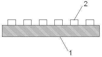
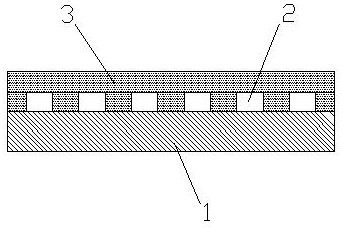
[0042] Embodiment 1: see Figure 1 to Figure 3 , a method for suppressing surface waves on a temperature-compensated layer of a temperature-compensated surface acoustic wave device, comprising the steps of:
[0043] 1) Cleaning the wafer 1; cleaning the wafer 1 with the existing conventional cleaning technology; wherein, the wafer 1 adopts a lithium tantalate single crystal or a lithium niobate single crystal piezoelectric wafer 1, so as to manufacture a temperature-compensated acoustic surface wave devices.
[0044] 2) Fabricate the metal chip 2 (metal interdigitated layer) of the surface acoustic wave device on the device surface of the wafer 1; in actual production, use the wet (including stripping) process technology route and the dry etching route to complete the production. It is a mature existing technology.
[0045] 3) Fabricate a temperature compensation layer 3 on the metal surface of the metal chip 2; the temperature compensation layer 3 uses silicon dioxide, fluo...
Embodiment 2
[0051] Example 2, see Figure 8 to Figure 11 , the difference from Example 1 is that in step 4),
[0052] a) First use a dicing machine (grinding wheel or laser, etc.) or dry etching to make grooves 5 on the surface of the temperature compensation layer 3 on the surface of the acoustic channel, wherein the grooves 5 are single grooves 5 or dense grooves 5; when opening When the groove 5 is a single groove 5, the groove 5 is located between the input and output ends of the surface acoustic wave device. When the groove 5 is a dense groove 5, the density is 0.1 to 100 times the propagation wavelength of the upper surface.
[0053] b) Then, on the upper surface of the temperature compensation layer 3, the sound-absorbing glue 4 with a thickness of 10nm to 100nm is fully coated on the surface of the acoustic channel by means of screen glue, glue dispenser glue, or glue spray machine spray glue; Glue 4 fills up slot 5 . During the production process, according to the set thickness...
Embodiment 3
[0054] Example 3, see Figure 12 , 13 , the difference from Examples 1 and 2 is that in step 4),
[0055] a) First use a dicing machine (grinding wheel or laser, etc.) or dry etching to make grooves 5 on the surface of the temperature compensation layer 3 on the surface of the acoustic channel, wherein the grooves 5 are single grooves 5 or dense grooves 5; when opening When the groove 5 is a single groove 5, the groove 5 is located between the input and output ends of the surface acoustic wave device. When the groove 5 is a dense groove 5, the density is 0.1 to 100 times the propagation wavelength of the upper surface.
[0056] b) Then, in the groove 5 on the upper surface of the temperature compensation layer 3, the sound-absorbing glue 4 with a thickness of 10nm to 100nm is coated by screen glue, glue dispenser glue or glue spraying machine spray glue, and the sound-absorbing glue 4 will The groove 5 is filled and its upper side protrudes beyond the temperature compensatio...
PUM
 Abstract
Description
Claims
Application Information
 - R&D
- Intellectual Property
- Life Sciences
- Materials
- Tech Scout
- Unparalleled Data Quality
- Higher Quality Content
- 60% Fewer Hallucinations
Browse by: Latest US Patents, China's latest patents, Technical Efficacy Thesaurus, Application Domain, Technology Topic, Popular Technical Reports.
© 2025 PatSnap. All rights reserved.Legal|Privacy policy|Modern Slavery Act Transparency Statement|Sitemap|About US| Contact US: help@patsnap.com


