A global exposure pixel unit and its preparation method

A pixel unit and global exposure technology, which is applied in the field of image sensors, can solve problems such as the inability to effectively reduce the readout noise of the pixel unit, affect the sensitivity of the pixel unit, and distort the stored signal, so as to reduce the readout noise, increase the capacitance value, and increase the area effect

Active Publication Date: 2021-06-15
CHENGDU LIGHT COLLECTOR TECH
View PDF6 Cites 0 Cited by
  • Summary
  • Abstract
  • Description
  • Claims
  • Application Information

AI Technical Summary

Problems solved by technology

After changing to the back-illuminated type, since the surrounding area of ​​the lower plate of the MOS capacitor is a silicon substrate, and the silicon substrate is light-transmitting, the incident light can enter the lower plate of the capacitor, causing distortion of the stored signal
[0006] at the same time as figure 1 As shown, the photodiode 2 for photosensitive pixel unit and the lower plate 12 of the MOS capacitor are located in the substrate 1 at the same time. In order to ensure the sensitivity of the pixel unit, we hope to increase the photosensitive area, that is, the area of ​​the photodiode 2 as much as possible, so the MOS capacitor The area of ​​the photodiode is limited, that is, the maximum capacitance value of the MOS capacitor is limited, and the readout noise of the pixel unit cannot be effectively reduced.
At the same time, the area of ​​the photodiode is also limited by the lower plate of the capacitor. The part of the silicon substrate area occupied by the lower plate of the MOS capacitor cannot be used for light sensing, thus affecting the sensitivity of the pixel unit.

Method used


Image

  • A global exposure pixel unit and its preparation method
  • A global exposure pixel unit and its preparation method
  • A global exposure pixel unit and its preparation method

Examples


Embodiment Construction

[0041] In order to make the purpose, technical solution and advantages of the present invention clearer, the specific implementation manners of the present invention will be further described in detail below in conjunction with the accompanying drawings.

[0042] A method for preparing a global exposure pixel unit provided by the present invention comprises the following steps:

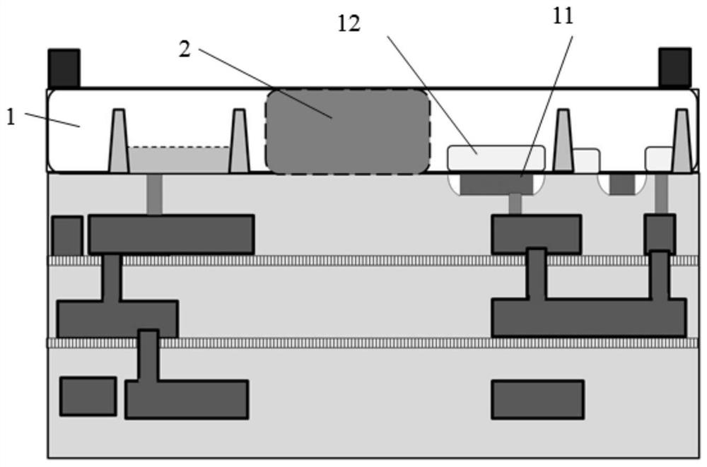
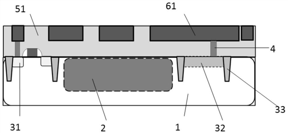
[0043] S01: If figure 2As shown, a substrate 1 is prepared, and a photodiode 2, a transistor 31 and an injection region 32 respectively located on both sides of the photodiode are formed in the substrate 1; a first dielectric layer 51 is deposited on the surface of the substrate 1, and the first dielectric layer A first metal layer 61 is formed in the layer, and the upper surface of the first metal layer 61 is flush with the upper surface of the first dielectric layer 51 ; the first metal layer 61 is interconnected with the transistor 31 and the injection region 32 through the contact hole 4 .

[00...


PUM

PropertyMeasurementUnit
thicknessaaaaaaaaaa
thicknessaaaaaaaaaa

Abstract

A global exposure pixel unit disclosed by the present invention includes a substrate and a dielectric layer region arranged in a vertical direction, the substrate includes a photodiode, transistors and injection regions respectively located on both sides of the photodiode; the dielectric layer region includes the first A dielectric layer, a second dielectric layer up to the Mth dielectric layer, and adjacent dielectric layers are separated by an etching barrier layer; the first dielectric layer, the second dielectric layer up to the Mth dielectric layer respectively contain a first metal layer , the second metal layer to the Mth metal layer; the trench metal located in the odd-numbered layer is connected to the source and drain of the transistor through the corresponding contact metal to form the upper plate of the storage capacitor, and the trench metal located in the even-numbered layer is connected to the source and drain of the transistor through the corresponding contact metal The injection region is connected to the lower electrode plate forming the storage capacitor to form the storage capacitor of the pixel unit. The global exposure pixel unit provided by the present invention increases the capacitance value of the storage capacitor, reduces the readout noise of the pixel unit, and improves the sensitivity of the pixel unit.

Description

technical field [0001] The invention relates to the field of image sensors, in particular to a global exposure pixel unit and a preparation method thereof. Background technique [0002] An image sensor refers to a device that converts optical signals into electrical signals. Large-scale commercial image sensor chips include charge-coupled device (CCD) image sensors and complementary metal-oxide semiconductor (CMOS) image sensor chips. Compared with traditional CCD image sensors, CMOS image sensors have the characteristics of low power consumption, low cost, and compatibility with CMOS technology, so they are more and more widely used. CMOS image sensors are now not only used in consumer electronics such as miniature digital cameras (DSC), mobile phone cameras, video cameras and digital single-lens reflex cameras (DSLR), but also in automotive electronics, monitoring, biotechnology and medical fields. [0003] In order to monitor high-speed objects, CMOS image sensors need t...

Claims


Application Information

Patent Timeline
Patent Type & Authority Patents(China)
IPC IPC(8): H01L27/146
CPCH01L27/14605H01L27/1463H01L27/14632H01L27/14634H01L27/14636H01L27/14687H01L27/1469
Inventor 王勇
Owner CHENGDU LIGHT COLLECTOR TECH
Why Eureka
Try Eureka