System-in-package module and terminal equipment
A technology of system-level packaging and plastic packaging, which is applied in the direction of semiconductor/solid-state device parts, semiconductor devices, electrical components, etc., can solve the complex dispensing process, poor interference shielding effect of packaging modules and external electronic components, and affect the shielding layer Covering effects and other issues to achieve the effect of ensuring the shielding effect and solving mutual electromagnetic interference
- Summary
- Abstract
- Description
- Claims
- Application Information
AI Technical Summary
Problems solved by technology
Method used
Image

Examples
Embodiment 1
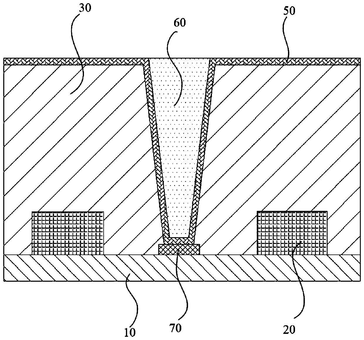
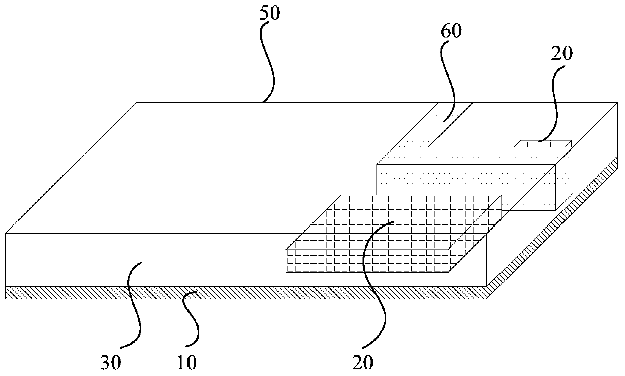
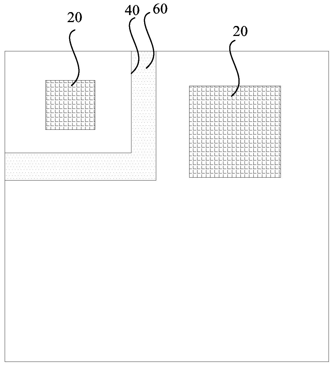
[0062] figure 1 is a schematic diagram of a partial cross-sectional structure of the system-in-package module provided in Embodiment 1 of the present application, figure 2 is a schematic diagram of the three-dimensional structure of the system-in-package module provided in Embodiment 1 of the present application, image 3 It is a schematic top view of the system-in-package module provided in Embodiment 1 of the present application, refer to Figure 1-Figure 3 As shown, Embodiment 1 of the present application provides a system-in-package module.
[0063] The system-in-package module provided by Embodiment 1 of the present application includes: a substrate 10 , at least two electronic components 20 , a plastic package 30 , a slot 40 , a conductive shielding layer 50 and a filler 60 . At least two electronic components 20 are disposed on the substrate 10 . The plastic package 30 is located on the substrate 10 and covers the surface of the substrate 10 , and at least two elect...
Embodiment 2
[0105] The system-in-package module provided by Embodiment 2 of the present application includes: a substrate 10 , at least two electronic components 20 , a plastic package 30 , a slot 40 , a conductive shielding layer 50 and a filler 60 . At least two electronic components 20 are disposed on the substrate 10 . The plastic package 30 is located on the substrate 10 and covers the surface of the substrate 10 , and at least two electronic components 20 are wrapped in the plastic package 30 . The slot 40 runs through the upper and lower surfaces of the plastic package 30 and takes the route between two adjacent electronic components 20 as a cutting path, or the slot 40 is located between two adjacent electronic components 20 . The conductive shielding layer 50 covers the upper surface of the plastic package 30 and the inner surface of the slot 40 . The filling body 60 fills the slot 40 .
[0106] Figure 11 is a schematic diagram of a partial cross-sectional structure of the sy...
Embodiment 3
[0130] Embodiment 3 of the present application provides a terminal device, including: the system-in-package module described in Embodiment 1 and Embodiment 2 above.
[0131] The terminal devices involved in Embodiment 3 of the present application may include electronic devices such as mobile phones, watches, tablet computers, personal digital assistants (Personal Digital Assistant, PDA), sales terminals (Point of Sales, POS), and vehicle-mounted computers.
[0132] The terminal equipment provided in this embodiment adopts a system-in-package module. The system-in-package module can solve the mutual electromagnetic interference between electronic components inside the system-in-package module by setting surface shielding and sub-cavity shielding. Solve the interference between the system-in-package module and external electronic components, realize the electromagnetic shielding effect between the internal electronic components to reach 20-30dB, and the electromagnetic shielding ...
PUM
| Property | Measurement | Unit |
|---|---|---|
| Size | aaaaa | aaaaa |
| Size | aaaaa | aaaaa |
| Thickness | aaaaa | aaaaa |
Abstract
Description
Claims
Application Information
 - R&D
- Intellectual Property
- Life Sciences
- Materials
- Tech Scout
- Unparalleled Data Quality
- Higher Quality Content
- 60% Fewer Hallucinations
Browse by: Latest US Patents, China's latest patents, Technical Efficacy Thesaurus, Application Domain, Technology Topic, Popular Technical Reports.
© 2025 PatSnap. All rights reserved.Legal|Privacy policy|Modern Slavery Act Transparency Statement|Sitemap|About US| Contact US: help@patsnap.com