
CMP method

A grinding method and technology of abrasives, applied in the field of CMP grinding, can solve the problems of particle defects on the surface of the silicon nitride layer, poor flatness of the silicon nitride layer, etc., and achieve the effects of increasing the grinding speed, flat coverage, and improving the residue of the abrasive.

Inactive Publication Date: 2020-01-14
WUHAN XINXIN SEMICON MFG CO LTD
View PDF9 Cites 0 Cited by
  • Summary
  • Abstract
  • Description
  • Claims
  • Application Information

AI Technical Summary

Problems solved by technology

The purpose of this process is to remove the redundant silicon oxide layer after filling by CMP, and stop at the silicon nitride layer. The flatness of the silicon nitride layer after CMP in the actual process is poor, and the particle defects on the surface of the silicon nitride layer are serious.

Method used


Image

  • CMP method
  • CMP method
  • CMP method

Examples


Embodiment Construction

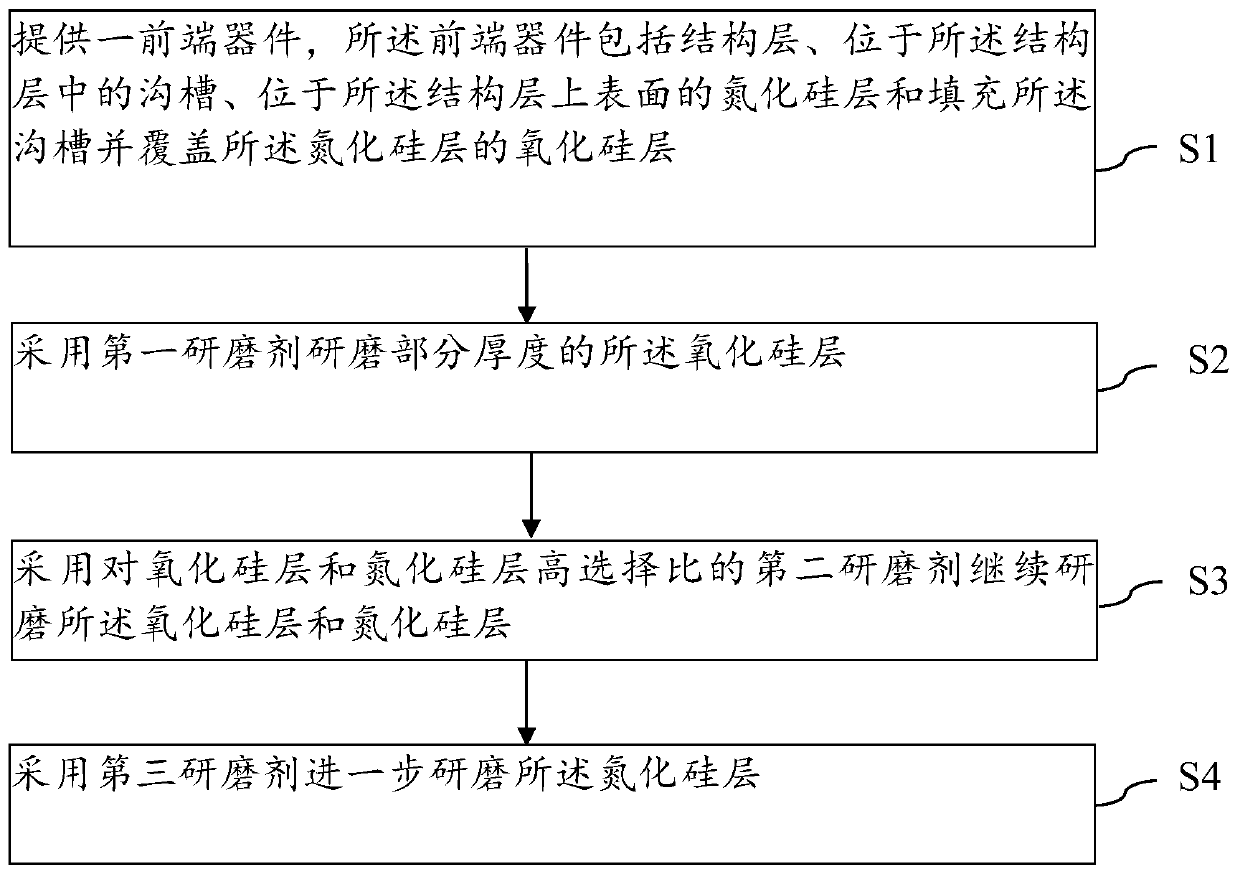
[0031] Based on the above research, an embodiment of the present invention provides a CMP grinding method. The present invention will be described in further detail below in conjunction with the accompanying drawings and specific embodiments. The advantages and features of the present invention will become clearer from the following description. It should be noted that the drawings are all in a very simplified form and use imprecise scales, and are only used to facilitate and clearly assist the purpose of illustrating the embodiments of the present invention.

[0032] The embodiment of the present invention provides a kind of CMP grinding method, such as figure 1 shown, including:

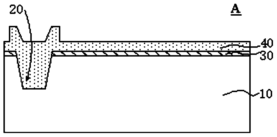
[0033] A front-end device is provided, and the front-end device includes a structural layer, a groove in the structural layer, a silicon nitride layer on the upper surface of the structural layer, and a silicon nitride layer that fills the groove and covers the silicon nitride layer. Silicon oxi...


PUM


Abstract

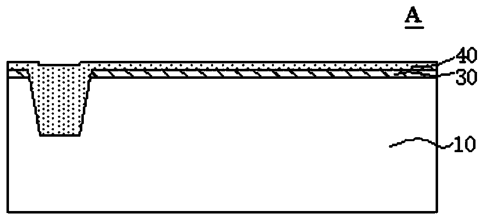
The invention provides a CMP (chemical mechanical polishing) method. The CMP method comprises the steps of: providing a front-end device which comprises a structural layer, a groove positioned in thestructural layer, a silicon nitride layer positioned on the upper surface of the structural layer and a silicon oxide layer for filling the groove and covering the silicon nitride layer; polishing thepart of the silicon oxide layer with a certain thickness by adopting a first polishing agent; polishing the silicon oxide layer and the silicon nitride layer by adopting a second polishing agent witha high selection ratio for the silicon oxide layer and the silicon nitride layer; and polishing the silicon nitride layer by adopting a third polishing agent so as to remove particle defects. The silicon oxide layer and the silicon nitride layer are polished through the second polishing agent with the high selection ratio for the silicon oxide layer and the silicon nitride layer, the flatness ofthe silicon nitride layer is improved, the silicon nitride layer is polished through the third polishing agent, and particle defects are removed.

Description

technical field [0001] The invention belongs to the technical field of integrated circuit manufacturing, and in particular relates to a CMP grinding method. Background technique [0002] Chemical mechanical polishing (CMP) is frequently used in the manufacturing process of semiconductor integrated circuits to achieve surface planarization of semiconductor devices. A high-quality CMP process is the guarantee for obtaining a flat surface of a semiconductor device. [0003] A semiconductor device such as an image sensor (CIS, Cmos Image Sensor) is formed with a groove, and a silicon nitride layer is formed on the surface of the semiconductor device, and the groove is filled with a silicon oxide layer, and the silicon oxide layer also extends to cover the silicon nitride layer. BSLR (Backside Layer Remove)-CMP is a process for grinding the silicon oxide layer and the silicon nitride layer above the groove in the image sensor (CIS, Cmos ImageSensor). The process is characterize...

Claims


Application Information

Patent Timeline
IPC IPC(8): H01L21/3105B24B37/04B24B37/10
CPCH01L21/31055B24B37/044B24B37/042B24B37/10
Inventor 杨一凡高志强
Owner WUHAN XINXIN SEMICON MFG CO LTD
Learn More