A kind of semiconductor structure and its manufacturing method
A manufacturing method and semiconductor technology, applied in semiconductor/solid-state device manufacturing, electrical components, circuits, etc., can solve the problems of DVC performance degradation, large graphic distortion, small process window, etc., to reduce film consumption, reduce contour deformation, The effect of reducing graphic distortion
- Summary
- Abstract
- Description
- Claims
- Application Information
AI Technical Summary
Problems solved by technology
Method used
Image

Examples
Embodiment 1
[0066] A method for fabricating a semiconductor structure is provided in this embodiment, please refer to Figure 4 , shown as a process flow diagram of the method, comprising the following steps:
[0067] S1: Provide a substrate, and form a hard mask laminate with a deposition temperature gradient in the thickness direction on the substrate, the hard mask laminate includes at least two hard mask layers, and the different hard masks The film layer corresponds to different deposition temperatures;
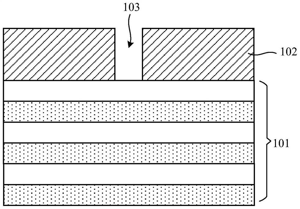
[0068] S2: forming an opening in the hard mask stack, the opening exposes the upper surface of the substrate, and the size of the top end of the opening is different from the size of the bottom end;
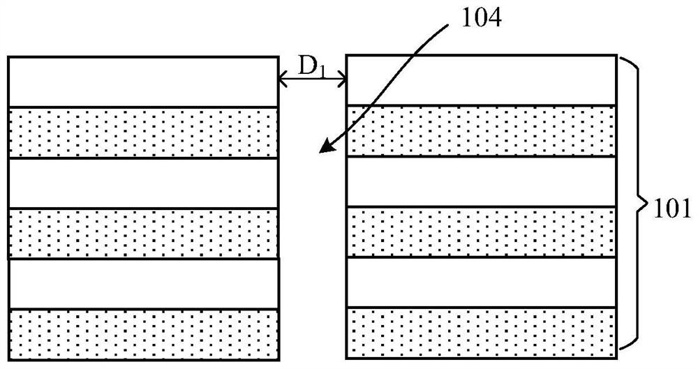
[0069] S3: Using the hard mask stack with the opening as a mask, forming a recess structure in the substrate.
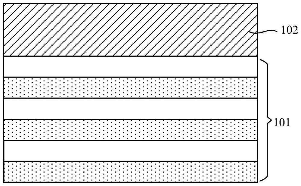
[0070] See first Figure 5 , performing step S1: providing a substrate 201, and forming a hard mask stack 202 with a deposition temperature gradient in the thickness direc...
Embodiment 2
[0084] This embodiment adopts basically the same technical solution as Embodiment 1, except that in Embodiment 1, the deposition temperature of the hard mask stack in the thickness direction decreases sequentially from bottom to top, and the width of the opening The gradient decreases from top to bottom, and in this embodiment, the deposition temperature of the hard mask stack in the thickness direction increases sequentially from bottom to top, and the width of at least one section of the opening gradually increases from top to bottom. Big.
[0085] see Figure 10 , performing step S1: providing a substrate 301, and forming a hard mask stack 302 on the substrate with deposition temperature gradients varying in the thickness direction.
[0086] Specifically, the substrate 301 can be a single-layer material or a multi-layer material, for example including Si layer, SiO 2 layer and at least one of SiN layer. In this embodiment, the substrate 301 includes two kinds of material...
Embodiment 3
[0099] This embodiment adopts basically the same technical solution as Embodiment 1 or Embodiment 2. The difference is that the same etching conditions are used in Embodiment 1 and Embodiment 2 to etch each of the hard mask stacks. A hard mask layer, the width of the opening changes in a gradient in the thickness direction, and in this embodiment, at least two sections of the opening adopt different etching conditions, wherein at least one section has a width in the thickness direction It has a gradient change, and the bottom section has a vertical side wall.
[0100] see Figure 15 , which is shown as the correlation result graph of hard mask (HM) density, hard mask opening critical dimension (CD) and hard mask deposition temperature, where DZ refers to heating with a dual zone heater (Dual Zone Heater). It can be seen from the figure that the density of HM is negatively correlated with the deposition temperature, and the CD of HMO is positively correlated with the depositio...
PUM
 Abstract
Description
Claims
Application Information
 - R&D
- Intellectual Property
- Life Sciences
- Materials
- Tech Scout
- Unparalleled Data Quality
- Higher Quality Content
- 60% Fewer Hallucinations
Browse by: Latest US Patents, China's latest patents, Technical Efficacy Thesaurus, Application Domain, Technology Topic, Popular Technical Reports.
© 2025 PatSnap. All rights reserved.Legal|Privacy policy|Modern Slavery Act Transparency Statement|Sitemap|About US| Contact US: help@patsnap.com