Low power on-chip rectifier bridge circuit

A low-power, rectifying bridge technology, applied in the direction of converting AC power input to DC power output, output power conversion devices, electrical components, etc., can solve the problems of high cost and power loss of rectification circuits, and achieve rectification efficiency and suppression Ringing phenomenon, the effect of reducing the output voltage drop

Pending Publication Date: 2019-12-06
WUXI LINLI SCI & TECH CO LTD
View PDF0 Cites 3 Cited by
  • Summary
  • Abstract
  • Description
  • Claims
  • Application Information

AI Technical Summary

Problems solved by technology

[0004] In view of the deficiencies in the background technology, the present invention provides a low-power on-chip rectifier bridge circuit. The technical problem to be solved is that the existing diode rectifier bridge circuit has a large power loss in operation due to the conduction voltage drop of the diode itself; The cost of rectification circuit combined with MOSFET and active rectifier bridge control chip is high

Method used


Image

  • Low power on-chip rectifier bridge circuit
  • Low power on-chip rectifier bridge circuit
  • Low power on-chip rectifier bridge circuit

Examples


Embodiment Construction

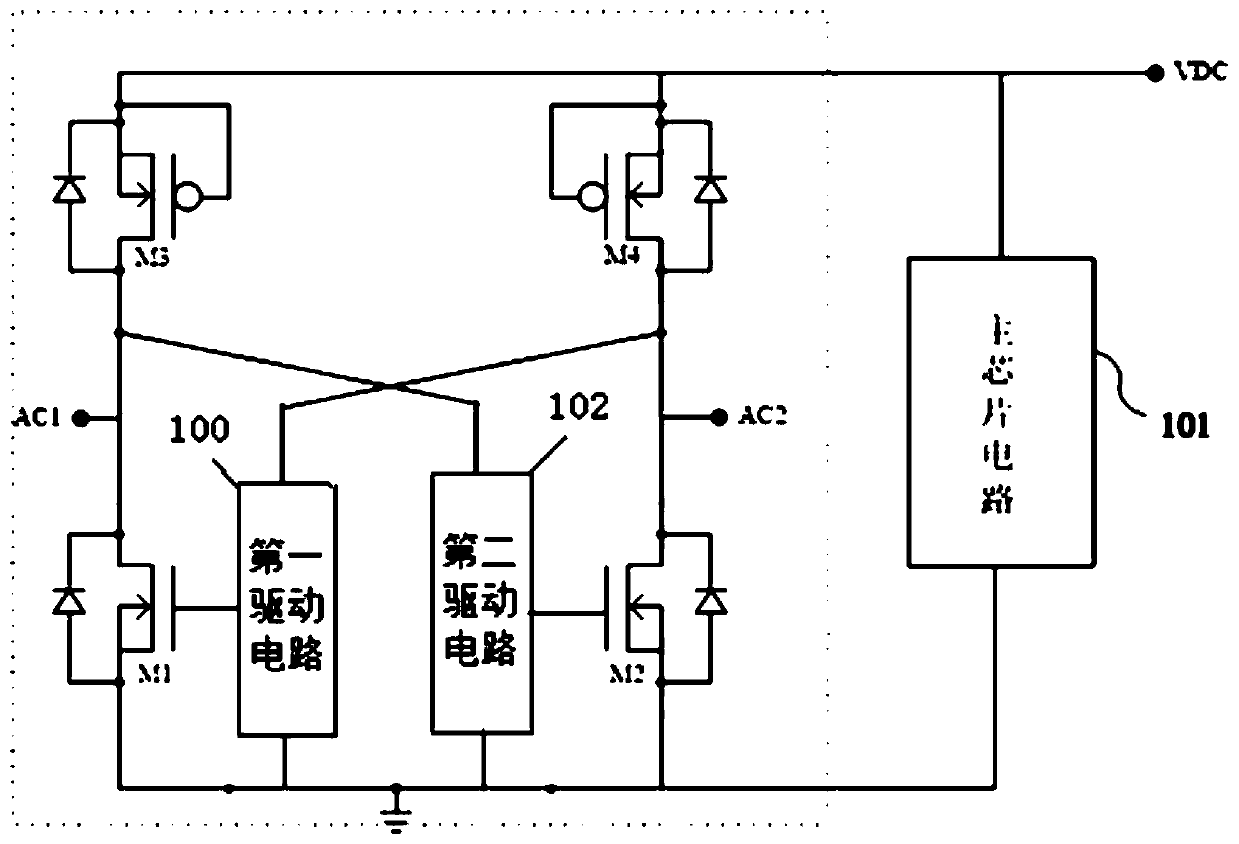
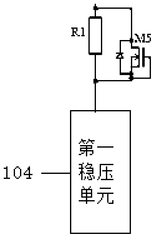
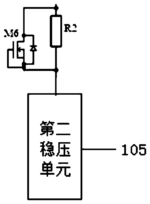
[0022] The present invention is described in further detail now in conjunction with accompanying drawing. These drawings are all simplified schematic diagrams, which only illustrate the basic structure of the present invention in a schematic manner, so they only show the configurations related to the present invention.

[0023] Such as Figure 1-4 As shown, the low-power on-chip rectifier bridge circuit includes a first NMOS transistor M1 , a second NMOS transistor M2 , a first PMOS transistor M3 , a second PMOS transistor M4 , a first drive control circuit 100 and a second drive control circuit 102 .

[0024] The gate and source of the first PMOS transistor M3 are short-circuited, the gate and source of the second PMOS transistor M4 are short-circuited, the source of the first PMOS transistor M3 is electrically connected to the source of the second PMOS transistor M4, and the first PMOS The drain of the transistor M3 is electrically connected to the drain of the first NMOS t...


PUM


Abstract

The invention relates to the field of rectifier circuits, and discloses a low power on-chip rectifier bridge circuit comprising a first NMOS transistor, a second NMOS transistor, a first PMOS transistor, a second PMOS transistor, a first drive control circuit and a second drive control circuit. The gate and the source of the first PMOS transistor are shorted. The gate and the source of the secondPMOS transistor are shorted. The source of the first PMOS transistor is electrically connected with the source of the second PMOS transistor. The drain of the first PMOS transistor is electrically connected with the drain of the first NMOS transistor. The drain of the second PMOS transistor is electrically connected with the drain of the second NMOS transistor. The source of the first NMOS transistor and the source of the second NMOS transistor are both grounded. The first drive control circuit controls the on-off of the first NMOS transistor. The second drive control circuit controls the on-off of the second NMOS transistor. The drain of the first NMOS transistor is electrically connected with a first AC input end. The drain of the second NMOS transistor is electrically connected with a second AC input end. The alternating current outputs DC signals through the first PMOS transistor or the second PMOS transistor so as to reduce voltage drop and improve rectification efficiency.

Description

technical field [0001] The invention relates to the field of rectifier circuits, in particular to a low-power on-chip rectifier bridge circuit. Background technique [0002] The traditional rectifier bridge circuit is mainly composed of four diodes, which use the unidirectional conduction characteristics of the diodes to rectify the AC power into a DC output, but there is a conduction voltage drop when the diodes are turned on, which is about 0.6V. Based on the rectification composed of multiple diodes There is a lot of power loss in the circuit, and it also makes the operating temperature rise. [0003] The rectification circuit combined with the switch MOSFET and the active rectifier bridge control chip utilizes the lower turn-on voltage drop of the switch tube MOSFET to improve the power loss problem caused by the inherent voltage drop of the diode. However, in this architecture, there are many defects in the use of separate devices and complicated PCB layout. At the sam...

Claims


Application Information

Patent Timeline
IPC IPC(8): H02M7/219
CPCH02M7/219H02M1/0054Y02B70/10
Inventor 赵寿全刘桂芝
Owner WUXI LINLI SCI & TECH CO LTD
Why Eureka
Try Eureka