Manufacturing method of three-dimensional memory

A manufacturing method and memory technology, applied in the direction of electric solid-state devices, semiconductor devices, electrical components, etc., can solve problems such as leakage, excessive etching, chip failure, etc., and achieve the effects of reducing manufacturing costs, improving efficiency, and high operability

Active Publication Date: 2019-12-06
YANGTZE MEMORY TECH CO LTD
View PDF4 Cites 4 Cited by
  • Summary
  • Abstract
  • Description
  • Claims
  • Application Information

AI Technical Summary

Problems solved by technology

It is difficult to ensure the shape of the bottom of the channel through hole through the existing etching process. It is often difficult to etch through the charge storage layer when etching the charge storage layer, resulting in the failure of the chip, or it is easy to cause excessive etching, resulting in the channel through hole. Conduction with surrounding devices, causing leakage, and the adjustment window of the etching process is getting smaller and smaller
The existing manufacturing process not only cannot guarantee the yield rate of 3D memory, but also increases the manufacturing cost of 3D memory virtually.

Method used


Image

  • Manufacturing method of three-dimensional memory
  • Manufacturing method of three-dimensional memory
  • Manufacturing method of three-dimensional memory

Examples


Embodiment Construction

[0043] The present invention will be described in detail below in conjunction with the accompanying drawings and specific embodiments. Note that the aspects described below in conjunction with the drawings and specific embodiments are only exemplary, and should not be construed as limiting the protection scope of the present invention.

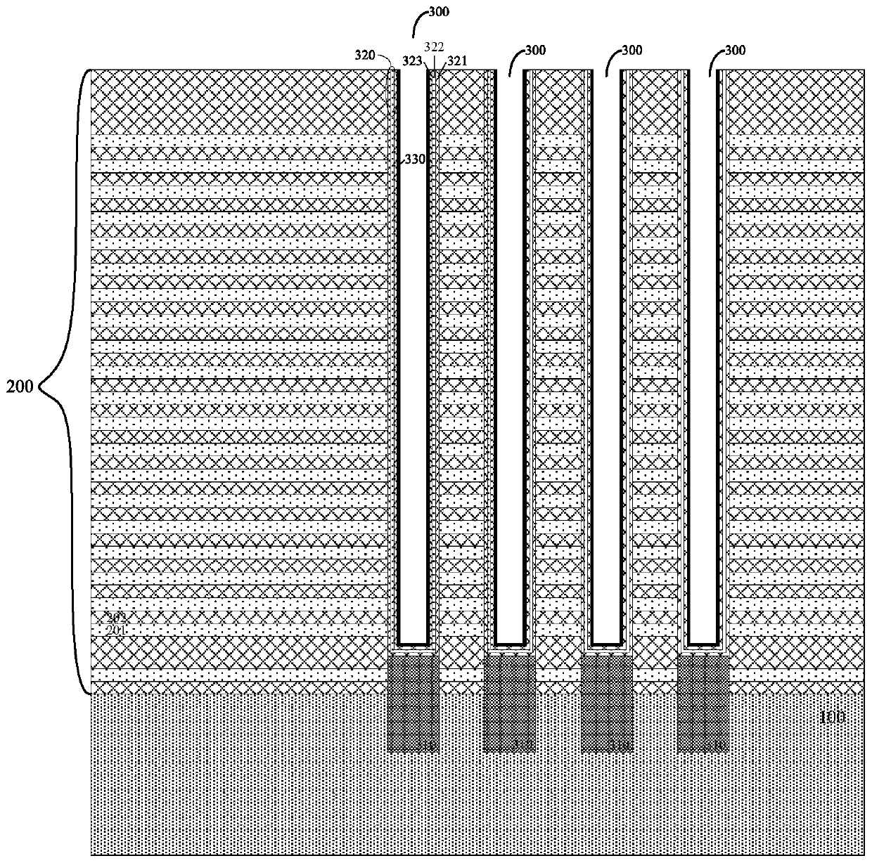
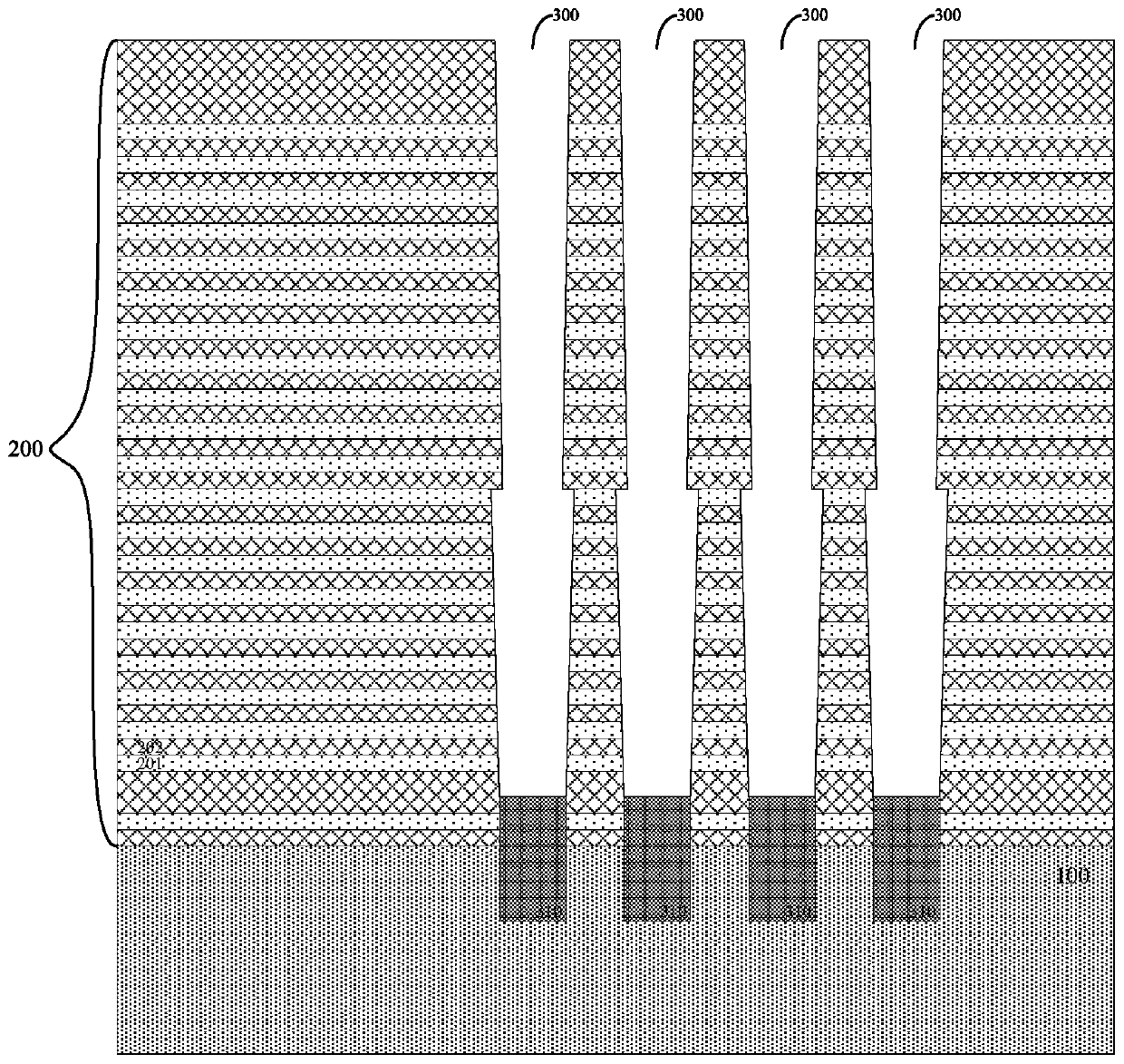
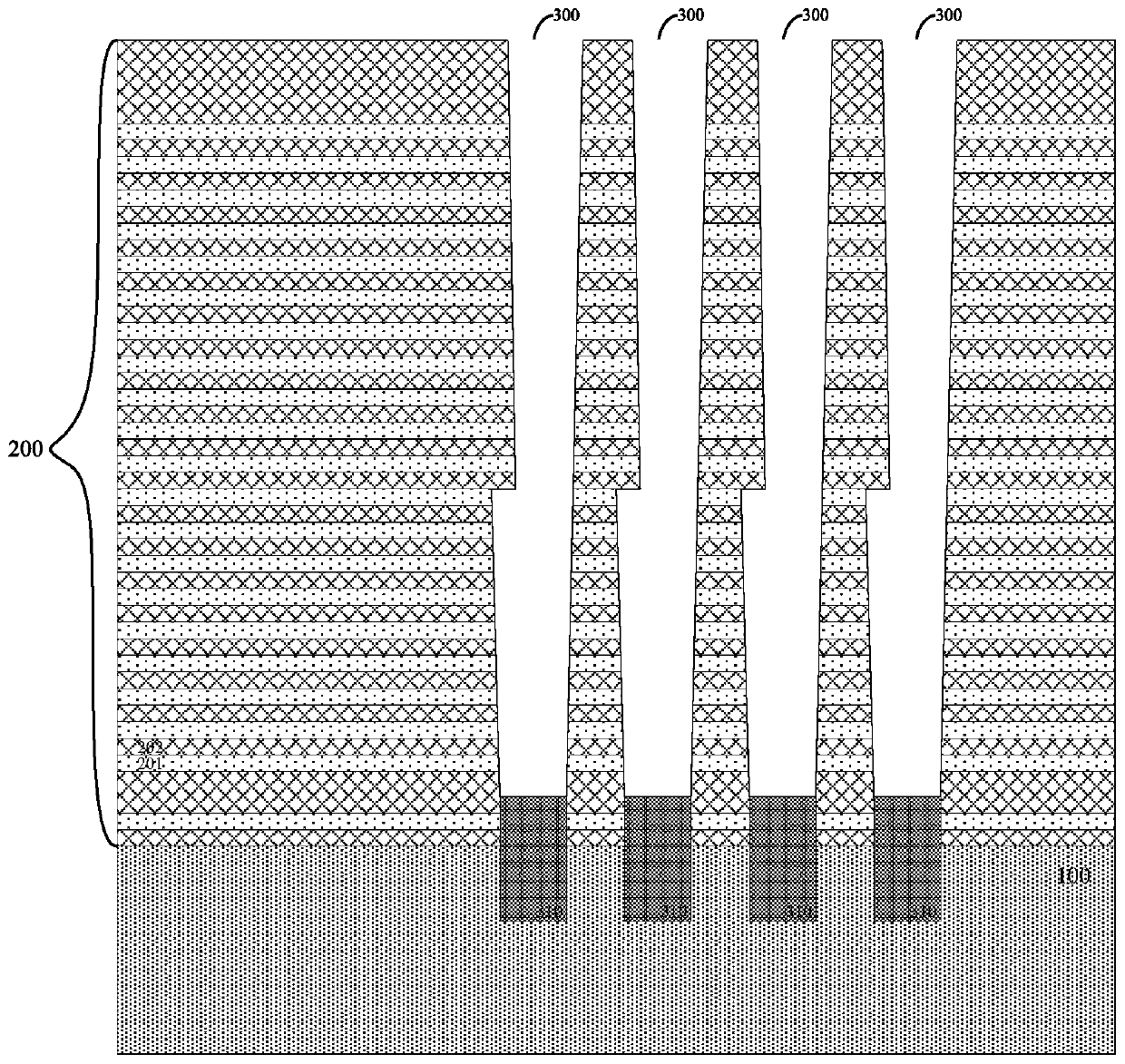
[0044] The present invention relates to semiconductor processing. More specifically, embodiments of the present invention provide a method for manufacturing a three-dimensional memory. The three-dimensional memory formed according to the manufacturing method provided by the present invention usually has higher stacking layers, so that the storage capacity can be expanded. In the case of storage capacity expansion, the manufacturing method provided by the present invention can ensure that the charge storage layer at the bottom of the three-dimensional memory channel hole has a good shape after etching, and the etching of the charge storage lay...


PUM


Abstract

The invention provides a manufacturing method of a three-dimensional memory. The method specifically comprises the steps: providing a substrate, wherein a channel through hole penetrating through a whole stacking layer in the height direction of the substrate is formed in the stacking layer on the substrate, a silicon epitaxial structure is formed at the bottom of the channel through hole, and a first oxide layer, a nitride layer, a second oxide layer and a protective layer are sequentially formed on the side wall of the channel through hole and the upper surface of the silicon epitaxial structure; etching the protective layer on the upper surface of the silicon epitaxial structure to form a notch exposing the second oxide layer; etching the second oxide layer through the gap by adopting afirst wet process; etching the nitride layer by adopting a second wet process; and etching the first oxide layer by using a third wet process to expose the silicon epitaxial structure, wherein the first wet process and the third wet process employ the same corrosive agent, which is different from the corrosive agent used in the second wet process. According to the manufacturing method provided bythe invention, the channel through hole bottom structure which does not influence surrounding devices can be formed so as to ensure good electrical characteristic performance of the devices.

Description

technical field [0001] The invention relates to the field of manufacturing semiconductor devices, in particular to a method for manufacturing a three-dimensional memory structure. Background technique [0002] In order to meet the development of high-efficiency and low-cost microelectronics industry, semiconductor memory devices need to have higher integration density. Regarding semiconductor memory devices, because their integration density is very important in determining product prices, that is, high-density integration is very important. For traditional two-dimensional and planar semiconductor storage devices, because their integration density mainly depends on the unit area occupied by a single storage device, the integration degree is very dependent on the quality of photolithography and masking process. However, even if expensive process equipment is continuously used to improve the precision of lithography and mask processes, the improvement of integration density i...

Claims


Application Information

Patent Timeline
Patent Type & Authority Applications(China)
IPC IPC(8): H01L27/11563H01L27/11578H01L27/11582H01L27/11568
CPCH10B43/00H10B43/30H10B43/20H10B43/27
Inventor 苏界顾立勋徐融孙文斌罗佳明
Owner YANGTZE MEMORY TECH CO LTD
Why Eureka
Try Eureka