Single-event latch-up protection device and latch-release method for charge measurement chip
A single-event latch and protective device technology, applied in the field of space electronics, can solve the problems of limited optional models, inoperability, and high price, and achieve the effect of quick recovery of work tasks
- Summary
- Abstract
- Description
- Claims
- Application Information
AI Technical Summary
Problems solved by technology
Method used
Image
Examples
Embodiment 1
[0030] A single event latch-up protection device for a charge measurement ASIC chip provided in this embodiment, the device includes:
[0031] A single event latch release device for automatically releasing the single event latch;
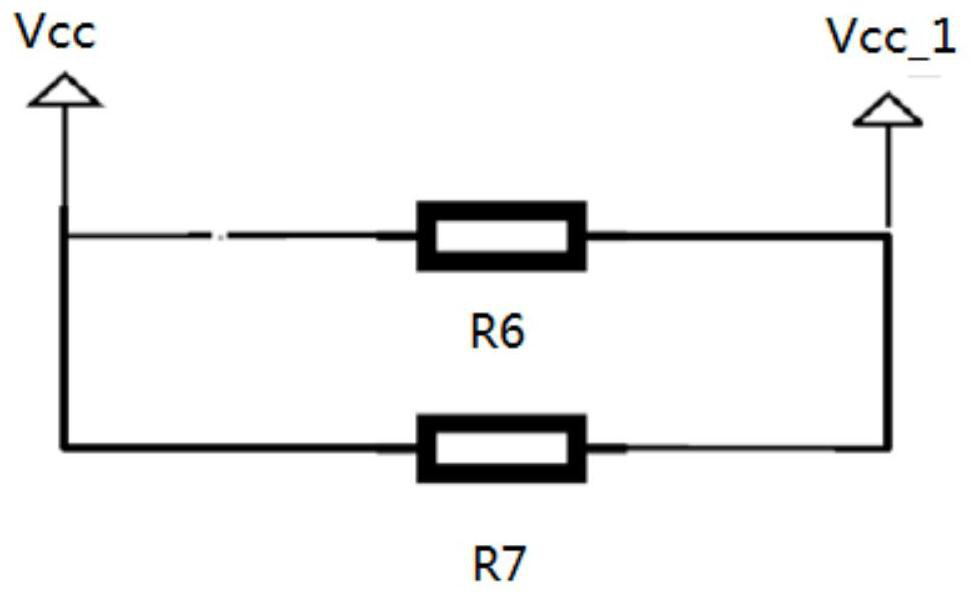
[0032] Single-event latch-up current limiter to suppress excessive latch-up current.
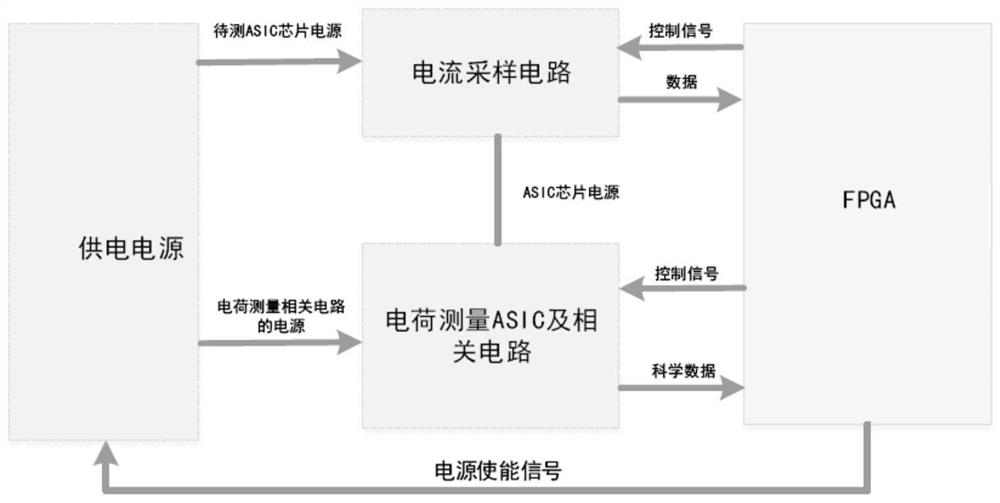
[0033] Specifically, such as figure 1 As shown, the single event latch release device consists of:
[0034] The power supply unit uses an independent LDO (Low Dropout Regulator, low dropout linear regulator) power supply chip to provide power supply for the charge measurement ASIC chip and related circuits, so that it does not affect the normal operation of other circuits on the board.
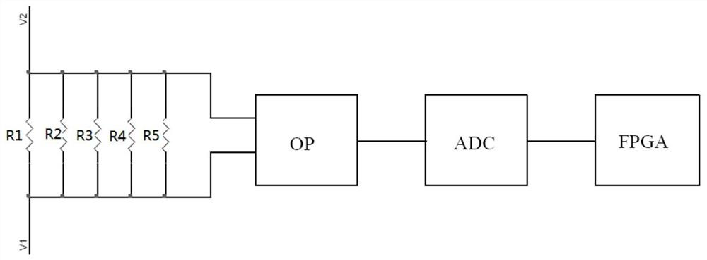
[0035] The current sampling circuit is used to sample the current of the power supply unit, wherein the current sampling circuit includes a current sampling probe, an operational amplifier OP and an analog-to-digital conversion device ADC, and the sampled power supply forms dif...
Embodiment 2
[0039] Such as Figure 4 As shown, the single event latch automatic release method of the charge measurement ASIC chip provided in this embodiment includes steps:
[0040] S1: The current sampling circuit samples the current of the power supply circuit of the power supply unit, and sends the sampled current value into the FPGA, and compares it with the preset current threshold. If the collected current is greater than the set threshold, it is considered as charge measurement The chip latches up;
[0041] S2: The FPGA outputs a low level to the control signal terminal of the charge measurement ASIC chip to prevent the existence of a sneak-through path during power failure. After an interval of 20ns, the interval time is taken as an example, not limited to this; The power enable signal turns off the LDO power supply chip in the power supply unit of the charge measurement related circuit. During the power failure, the FPGA sets the power failure status register and starts the po...
PUM
 Abstract
Description
Claims
Application Information
 - R&D
- Intellectual Property
- Life Sciences
- Materials
- Tech Scout
- Unparalleled Data Quality
- Higher Quality Content
- 60% Fewer Hallucinations
Browse by: Latest US Patents, China's latest patents, Technical Efficacy Thesaurus, Application Domain, Technology Topic, Popular Technical Reports.
© 2025 PatSnap. All rights reserved.Legal|Privacy policy|Modern Slavery Act Transparency Statement|Sitemap|About US| Contact US: help@patsnap.com


