
Optical sensor, optical sensing system and manufacturing method thereof

An optical sensor and sensing technology, applied in the field of optical sensors, can solve the problems of high power consumption, heavy use of batteries, and the inability of mobile phone batteries to last for a long time, and achieve the effect of reducing thickness and eliminating stray light.

Pending Publication Date: 2019-11-19
EGIS TECH
View PDF0 Cites 14 Cited by
  • Summary
  • Abstract
  • Description
  • Claims
  • Application Information

AI Technical Summary

Problems solved by technology

For this reason, the battery of the mobile phone cannot have a long service time
And because the new 5G mobile phones will consume more power in the future, the use of batteries is even more preoccupied.

Method used


Image

  • Optical sensor, optical sensing system and manufacturing method thereof
  • Optical sensor, optical sensing system and manufacturing method thereof
  • Optical sensor, optical sensing system and manufacturing method thereof

Examples


Embodiment Construction

[0161] The following disclosure provides many embodiments or examples, and specific examples of each element and its configuration are described below to simplify the description of the embodiments of the present invention. Of course, these are just examples, not intended to limit the embodiments of the present invention. For example, if a description mentions that a first element is formed on a second element, it may include an embodiment in which the first and second elements are in direct contact, or may include an additional element formed between the first and second elements , so that they are not in direct contact with the example. In addition, the embodiments of the present invention may repeat reference numerals and / or letters in different examples. This repetition is for brevity and clarity rather than to show the relationship between the different embodiments discussed.

[0162] In addition, spatial relative terms such as "below", "beneath", "lower", "above", "hig...


PUM


Abstract

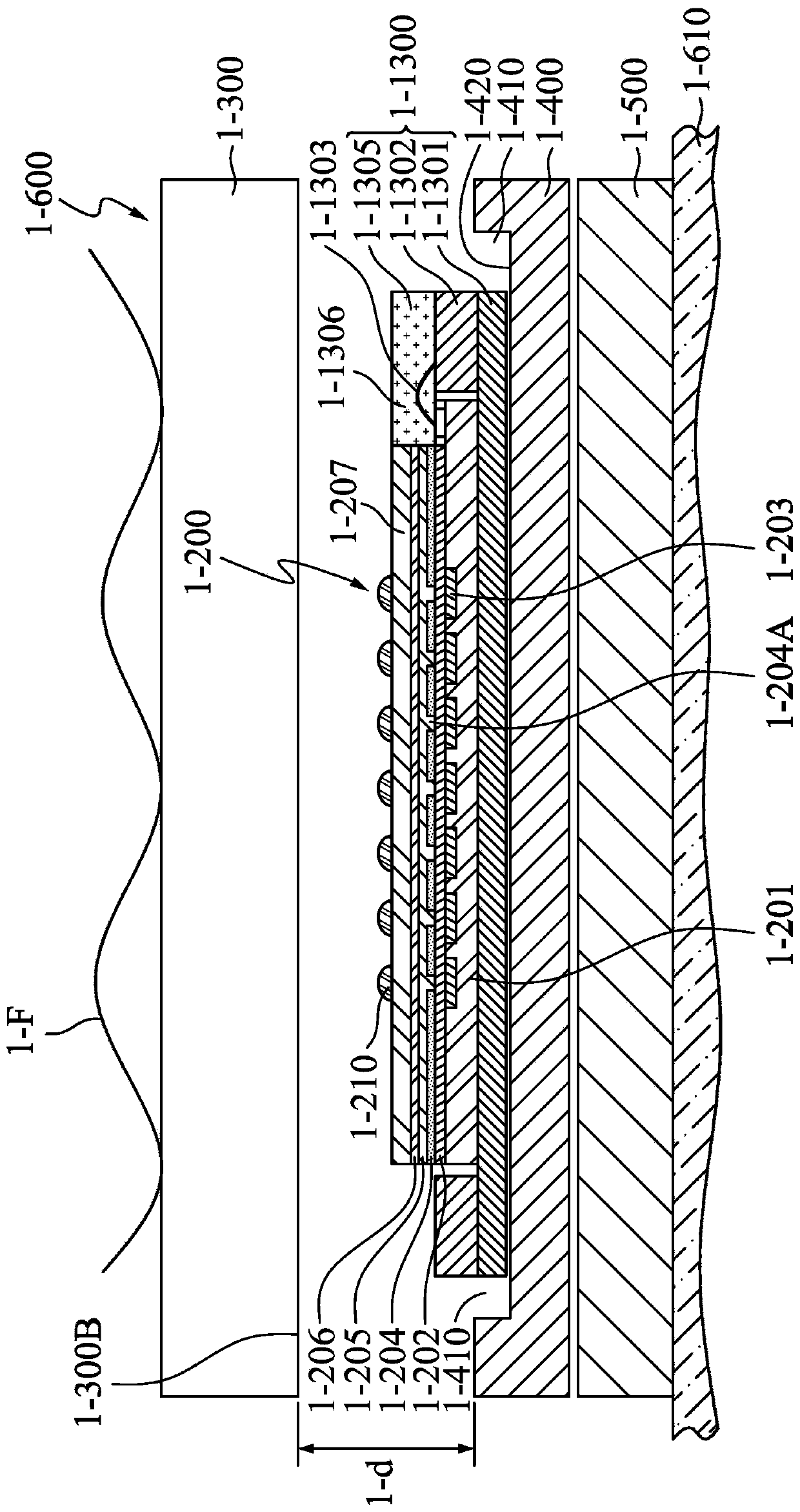
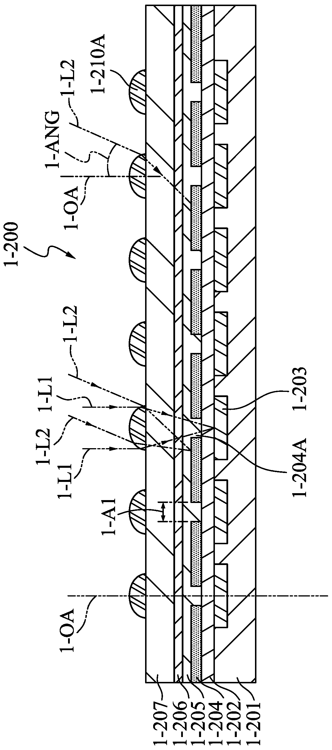
The invention provides an optical sensor, an optical sensing system and a manufacturing method thereof. The optical sensor includes: a substrate having a plurality of sensing pixels arranged in an array; the first transparent dielectric layer is positioned above the substrate; and a plurality of microlenses arranged in an array and located on or above the first transparent dielectric layer. The micro lenses enable a plurality of parallel forward incident light entering the micro lenses from the outside to pass through the first transparent dielectric layer to be incident into part or all of the total number of the sensing pixels. And a plurality of parallel oblique incident light entering the micro lens from the outside is incident to the outside of a part or all of the total number of thesensing pixels, so that the image of the target object is sensed. The target object generates parallel forward incident light and parallel oblique incident light, the forward incident light is parallel to a plurality of optical axes of the micro lens, and an angle is formed between each oblique incident light and each optical axis. The invention also provides an optical sensing system using the optical sensor and a manufacturing method of the optical sensor.

Description

technical field [0001] The present invention relates to an optical sensor (sensor), an optical sensor system and a manufacturing method thereof, in particular to an optical sensor with an angle controllable collimator structure (Angle Controllable Collimator), and an optical sensor using the optical sensor Sensing system and method of manufacture thereof. Background technique [0002] Today's mobile electronic devices (such as mobile phones, tablets, laptops, etc.) are usually equipped with user biometric systems, including different technologies such as fingerprints, faces, irises, etc., to protect personal data security, such as mobile phones Portable devices such as smart watches or smart watches also have the function of mobile payment, and it has become a standard function for user biometrics, while the development of portable devices such as mobile phones is moving towards full screen (or ultra-narrow bezel ), the trend of traditional capacitive fingerprint keys (such...

Claims


Application Information

Patent Timeline
Patent Type & Authority Applications(China)
IPC IPC(8): H01L27/146
CPCH01L27/14627H01L27/14634H01L27/14621H01L27/14623H01L27/146
Inventor 范成至黄振昌傅同龙黄郁湘
Owner EGIS TECH
Learn More