Processing apparatus

A processing device and processing unit technology, which is applied in the manufacture of electrical components, manipulators, semiconductors/solid-state devices, etc., can solve the problems that the ordering party cannot predict in advance and cannot grasp where the process is going.

Pending Publication Date: 2019-10-25
DISCO CORP
View PDF9 Cites 0 Cited by
  • Summary
  • Abstract
  • Description
  • Claims
  • Application Information

AI Technical Summary

Problems solved by technology

[0005] When manufacturing a semiconductor device through the above-mentioned multiple processes, the orderer who ordered the manufacture of the device chip cannot grasp where the process has progressed until the delivery date
Therefore, even if there is a delay in the delivery of the product, the ordering party cannot predict in advance

Method used


Image

  • Processing apparatus
  • Processing apparatus
  • Processing apparatus

Examples


Embodiment approach 1

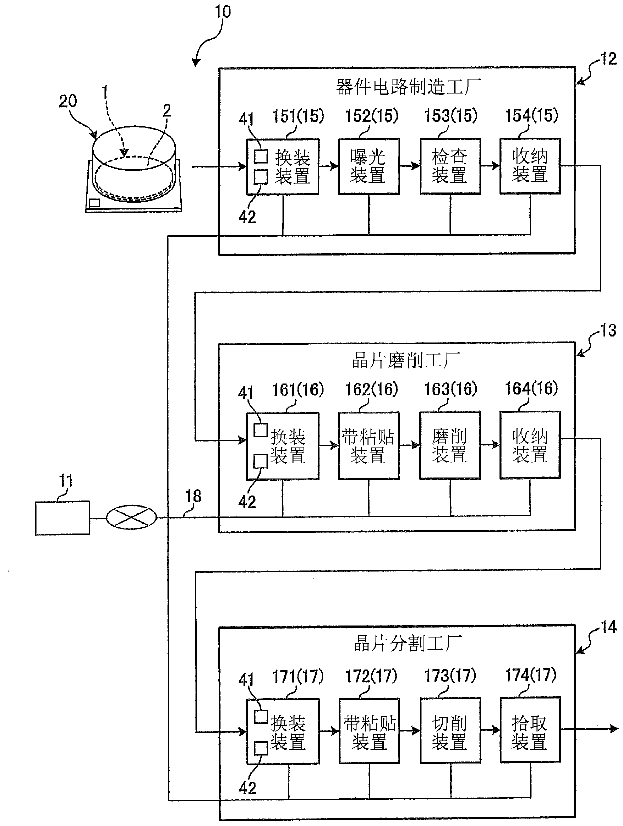
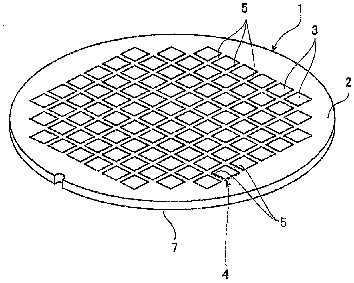
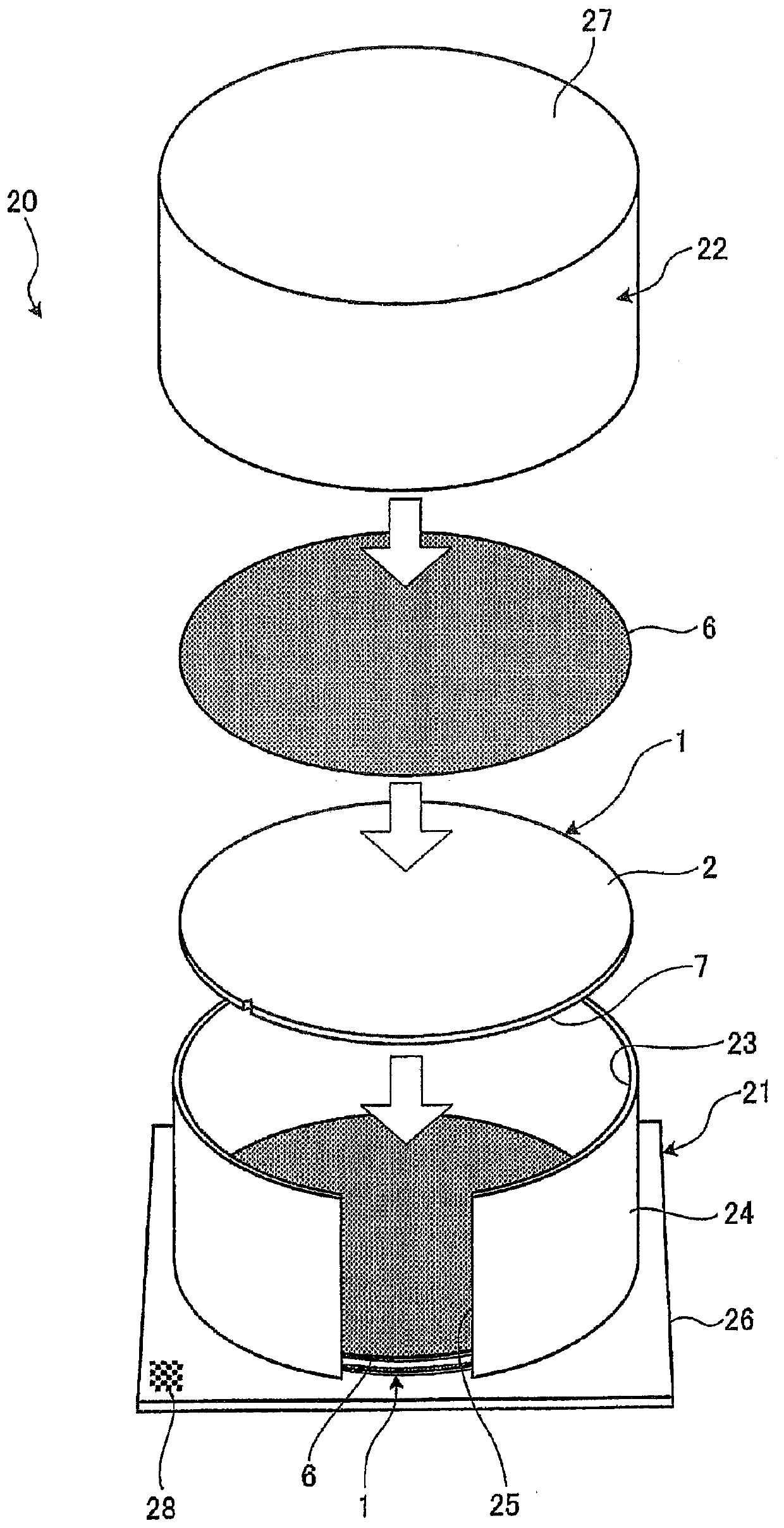
[0020] A processing device according to Embodiment 1 of the present invention will be described with reference to the drawings. figure 1 It is a figure which shows the device chip manufacturing factory provided with the replacement apparatus which is an example of the processing apparatus of Embodiment 1. figure 2 is showing figure 1 A perspective view of a workpiece to be processed in the device chip manufacturing factory shown. image 3 is showing the right to move into figure 1 A perspective view of an example of a coin stacker for storing workpieces in the device chip manufacturing factory shown. Figure 4 is shown in figure 1 A perspective view of an example of a processing cartridge used in the device chip manufacturing factory shown.

[0021] (device chip manufacturing plant)

[0022] figure 1 The shown device chip manufacturing factory 10 is on the front side 2 of the workpiece 1 as figure 2 After the device 3 is formed as shown, the workpiece 1 is divided int...


PUM


Abstract

A processing device is provided so that a consumer who orders the processing of a workpiece can grasp the progress of the process. The processing apparatus includes a cassette mounting section mounting a cassette storing a plurality of workpieces, a reading section reading an identification code provided on the cassette mounted on the cassette mounting section, and an information transmitting section transmitting information on the progress of process steps in processing each workpiece stored in the cassette, to a customer that has ordered the processing of each workpiece stored in the cassette.

Description

technical field [0001] The invention relates to processing devices. Background technique [0002] Areas with semiconductor devices or various functions are demarcated on the plate-shaped workpiece by dividing planned lines. In the manufacturing process of processing the workpiece and dividing it into individual device chips, multiple processing devices (processing device) for processing (processing) (for example, refer to Patent Document 1 and Patent Document 2). For example, in the case of a semiconductor device, a process of manufacturing a wafer, a process of forming a device on the wafer, and a process of thinning or dividing the wafer are performed. Usually these processes are carried out in different factories respectively. [0003] Patent Document 1: Japanese Patent Laid-Open No. 2005-045033 [0004] Patent Document 2: Japanese Patent Laid-Open No. 2017-11178 [0005] When a semiconductor device is manufactured through a plurality of processes as described above, ...

Claims


Application Information

Patent Timeline
Patent Type & Authority Applications(China)
IPC IPC(8): H01L21/67
CPCH01L21/67294H01L21/67276H01L21/6838H01L21/67766H01L21/67778B25J15/06H01L21/67309H01L21/67092H01L21/67742H01L21/6773
Inventor 关家一马
Owner DISCO CORP
Why Eureka
Try Eureka