
A kind of preparation method of double-layer structure silicon epitaxial wafer

A silicon epitaxial wafer, double-layer structure technology, used in semiconductor/solid-state device manufacturing, electrical components, circuits, etc., can solve the problem of large gap between double-layer silicon epitaxial wafers, slow rise of resistivity between layers, and consistency of intra-chip resistivity Difficult to control and other problems, to achieve the effect of improving the climb rate and satisfying the effective thickness

Active Publication Date: 2021-04-09
CHINA ELECTRONICS TECH GRP NO 46 RES INST
View PDF6 Cites 0 Cited by
  • Summary
  • Abstract
  • Description
  • Claims
  • Application Information

AI Technical Summary

Problems solved by technology

[0003] The purpose of the present invention is to overcome the large difference in resistivity design index between the first layer and the second layer silicon epitaxial layer used in the existing discrete devices such as Schottky diodes and fast recovery diodes, resulting in the in-chip resistivity Consistency is difficult to control, and the interlayer resistivity climbs slowly. A method for preparing a double-layer silicon epitaxial wafer is developed to improve the consistency of the resistivity distribution in the chip and the interlayer resistivity climb rate.

Method used


Image

  • A kind of preparation method of double-layer structure silicon epitaxial wafer
  • A kind of preparation method of double-layer structure silicon epitaxial wafer
  • A kind of preparation method of double-layer structure silicon epitaxial wafer

Examples


Embodiment 1

[0037] (1) Hydrogen chloride gas was introduced into the reaction chamber, and the flow rate of hydrogen chloride gas was set at 18 L / min. The residual deposition material on the graphite base of the reaction chamber was etched at high temperature, and the reaction temperature was set at 1180°C. The time was set at 1.0 min.

[0038] (2) Set the flow rate of hydrogen in the main process to 75 L / min, carry gaseous trichlorosilane into the reaction chamber, set the flow rate of trichlorosilane to 13.5 L / min, and set the deposition time to 20 sec. A layer of non-doped dense polysilicon is deposited on the surface of the seat.

[0039] (3) Load the silicon substrate on the disc-type base in the reaction chamber, and raise the temperature to 1160°C.

[0040] (4) Pass in hydrogen chloride gas, the flow rate of hydrogen chloride gas is set to 0.8 L / min, and the surface of the silicon substrate is polished, the polishing time is set to 1.0 min, and then the temperature is lowered to 1...

Embodiment 2

[0049] (1) Hydrogen chloride gas was introduced into the reaction chamber, and the flow rate of hydrogen chloride gas was set to 18 L / min. The residual deposited substances on the graphite base of the reaction chamber were etched at high temperature, and the reaction temperature was set to 1180 °C. The eclipse time was set to 1.0 min.

[0050] (2) Set the flow rate of hydrogen in the main process to 75 L / min, carry gaseous trichlorosilane into the reaction chamber, set the flow rate of trichlorosilane to 13.5 L / min, and set the deposition time to 20 sec. A layer of non-doped dense polysilicon is deposited on the surface of the seat.

[0051] (3) Load the silicon substrate on the disc-type base in the reaction chamber, and raise the temperature to 1160°C.

[0052] (4) Pass in hydrogen chloride gas, the flow rate of hydrogen chloride gas is set to 2.0 L / min, and the surface of the silicon substrate is polished, the polishing time is set to 1.0 min, and then the temperature is l...


PUM

PropertyMeasurementUnit
diameteraaaaaaaaaa
electrical resistivityaaaaaaaaaa
thicknessaaaaaaaaaa

Abstract

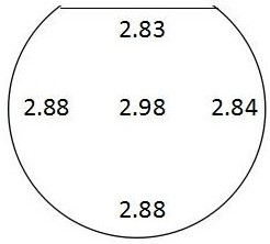
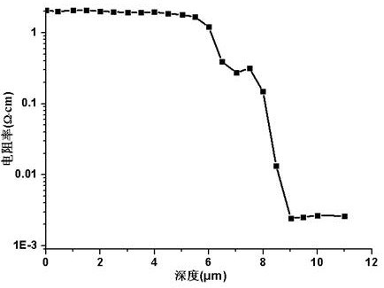
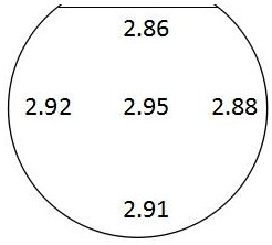
The invention discloses a method for preparing a double-layer structure silicon epitaxial wafer. This method realizes the control of the resistivity and uniformity of the silicon epitaxial layer by pre-depositing dense polysilicon on the base, adjusting the proportion of phosphine gas, the main process hydrogen flow, the base rotation speed, and the Slit hydrogen flow. The non-uniformity within the chip has been improved from more than 2.0% to less than 0.8%. At the same time, by designing the growth process of the buffer layer, the vertical resistivity climbing rate of the second silicon epitaxial layer has been improved, ensuring that the silicon epitaxial The effective thickness of the layer meets the design requirements.

Description

technical field [0001] The invention relates to the preparation technology of semiconductor epitaxial materials, in particular to a preparation method of a double-layer structure silicon epitaxial wafer. Background technique [0002] Traditional Schottky diodes, fast recovery diodes and other dies use breakdown voltage, forward conduction voltage, and anti-static interference (ESD) as the main evaluation parameters. The silicon epitaxial material used is usually a single-layer silicon epitaxial wafer. The silicon substrate layer and the silicon epitaxial layer are composed of two parts. As the base material for realizing key electrical characteristics, there is a certain doping ratio between the silicon substrate layer and the silicon epitaxial layer, that is, the silicon substrate layer with low resistivity and the silicon epitaxial layer with high resistivity. However, for such Schottky diodes and fast recovery diodes, the breakdown voltage and forward conduction voltage ...

Claims


Application Information

Patent Timeline
Patent Type & Authority Patents(China)
IPC IPC(8): H01L21/02H01L21/67
CPCH01L21/02381H01L21/0245H01L21/02513H01L21/02532H01L21/0259H01L21/0262H01L21/67253H01L21/67276
Inventor 周幸李明达王楠赵扬李普生
Owner CHINA ELECTRONICS TECH GRP NO 46 RES INST
Learn More