Anti-electromagnetic interference substrate and preparation method thereof, and electronic equipment

An anti-electromagnetic interference and substrate technology, applied in the field of electronics, can solve the problems of abnormal bonding between copper film and substrate, increase cost, waste, etc., and achieve the effect of facilitating automated mass production, reducing waste and ensuring quality.

Inactive Publication Date: 2019-10-15
OPPO CHONGQING INTELLIGENT TECH CO LTD
View PDF6 Cites 0 Cited by
  • Summary
  • Abstract
  • Description
  • Claims
  • Application Information

AI Technical Summary

Problems solved by technology
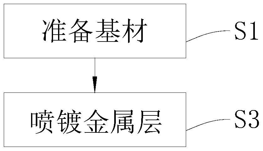
[0003] The purpose of the embodiments of the present application is to provide a method for preparing an anti-electromagnetic interference substrate to solve the problem in the prior art that the operation of manually pasting the copper film on the substrate is relatively frequent, which may easily cause abnormal bonding between the copper film and the substrate, resulting in waste , the problem of increasing cost

Method used


Image

  • Anti-electromagnetic interference substrate and preparation method thereof, and electronic equipment
  • Anti-electromagnetic interference substrate and preparation method thereof, and electronic equipment
  • Anti-electromagnetic interference substrate and preparation method thereof, and electronic equipment

Examples


Embodiment Construction

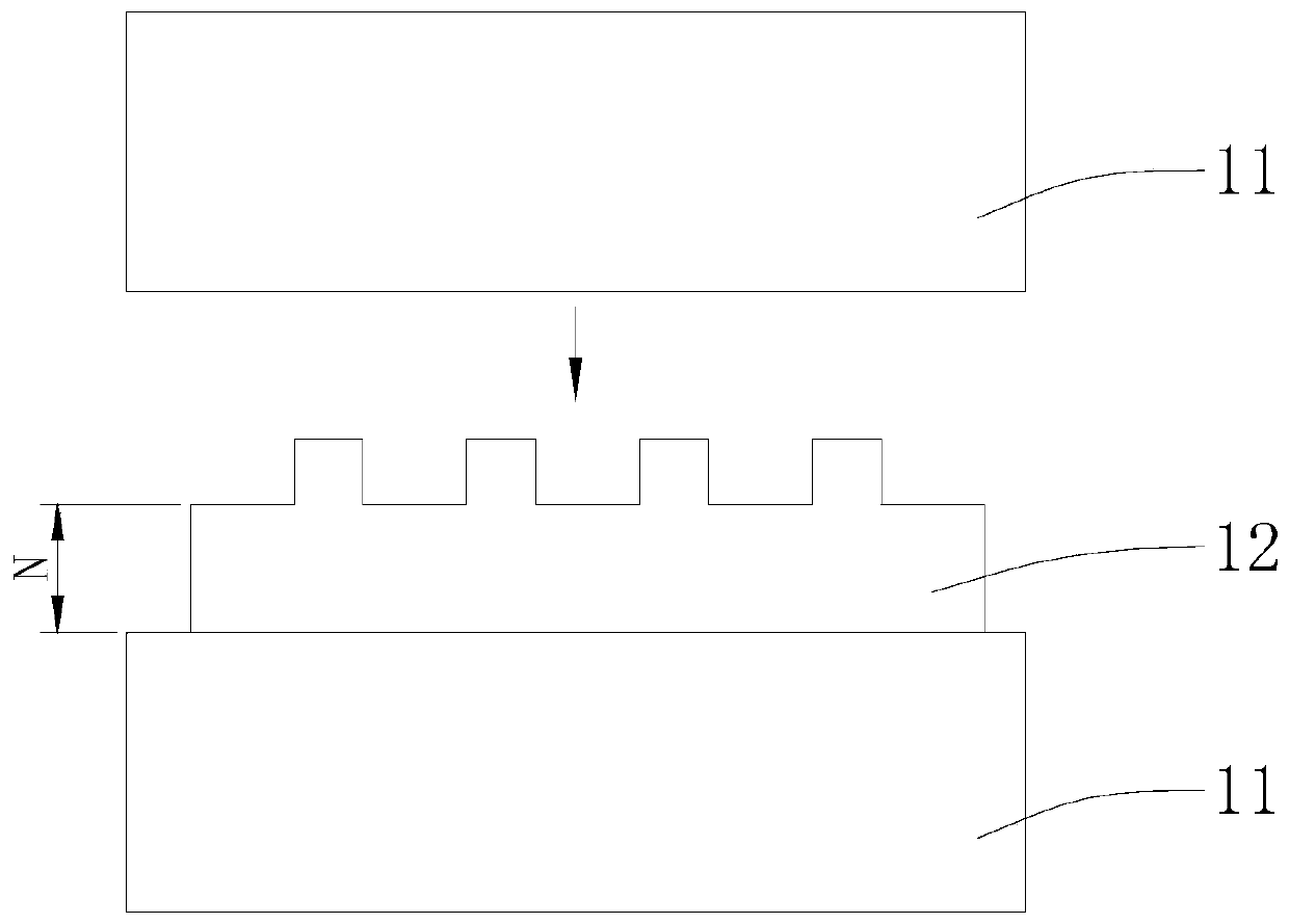
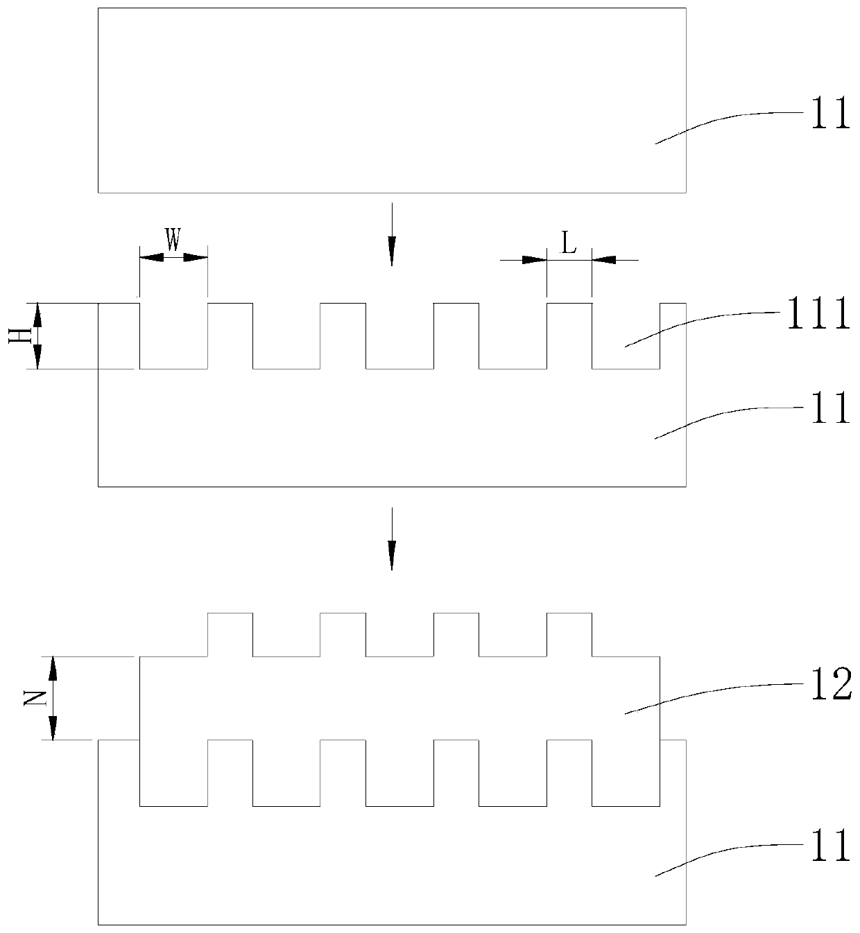
[0045] In order to make the technical problems, technical solutions and beneficial effects to be solved by the present application clearer, the present application will be further described in detail below in conjunction with the accompanying drawings and embodiments. It should be understood that the specific embodiments described here are only used to explain the present application, and are not intended to limit the present application.

[0046] It should be noted that when an element is referred to as being “fixed” or “disposed on” another element, it may be directly on the other element or be indirectly on the other element. When an element is referred to as being "connected to" another element, it can be directly connected to the other element or indirectly connected to the other element.

[0047] In addition, the terms "first" and "second" are used for descriptive purposes only, and cannot be interpreted as indicating or implying relative importance or implicitly specify...


PUM

PropertyMeasurementUnit
thicknessaaaaaaaaaa

Abstract

The invention provides an anti-electromagnetic interference substrate and a preparation method thereof, and electronic equipment. The preparation method of the anti-electromagnetic interference substrate comprises the following steps that a base material is provided, and a shielding area needing to be provided with electromagnetic shielding on the base material is determined; metal particles are sprayed on the shielding area of the base material, and thus a metal coating is formed on the shielding area; and the metal particles are one of copper particles, silver particles, gold particles, copper alloy, silver alloy or gold alloy. The metal coating on the shielding area of the base material by spraying one of copper particles, silver particles, gold particles, copper alloy, silver alloy orgold alloy, so that the shielding area can provide good electromagnetic shielding protection; moreover, the quality of the metal coating can be ensured, automatic mass production can be conducted conveniently, manual sticking is not needed, abnormal fitting is avoided, and waste is reduced; and the method is particularly applicable to a substrate with a complicated and sharp surface, and the adaptability is good.

Description

technical field [0001] The application belongs to the field of electronic technology, and more specifically relates to an anti-electromagnetic interference substrate, a preparation method thereof, and electronic equipment. Background technique [0002] At present, with the rapid development of communication technology, magnetic fields and electromagnetic waves surround people's environment, and various electronic equipment and electrical equipment are also in such an environment. Therefore, it is necessary to shield the interference of such magnetic fields and electromagnetic waves on equipment to ensure normal information transmission and avoid bad information generated. At present, the method commonly used to shield electromagnetic signal interference is generally to directly paste copper foil or copper-plated diaphragm, and use the conductive layer constructed by it to shield the interference of electromagnetic signals to electronic devices. However, due to the softness ...

Claims


Application Information

Patent Timeline
Patent Type & Authority Applications(China)
IPC IPC(8): C23C4/131C23C4/08C23C4/02C23C4/01H05K9/00
CPCC23C4/02C23C4/08C23C4/01C23C4/131H05K9/0084
Inventor 杨光明侯体波黄志勇
Owner OPPO CHONGQING INTELLIGENT TECH CO LTD
Why Eureka
Try Eureka