Non-volatile memory reading circuit and reading method
What is Al technical title?
Al technical title is built by PatSnap Al team. It summarizes the technical point description of the patent document.
A technology of non-volatile memory and readout circuit, which is applied in the field of integrated circuits and can solve the problems of long readout time and large dynamic power consumption of non-volatile memory
Active Publication Date: 2019-09-27
SHANGHAI INST OF MICROSYSTEM & INFORMATION TECH CHINESE ACAD OF SCI
View PDF4 Cites 2 Cited by
Summary
Abstract
Description
Claims
Application Information
AI Technical Summary
This helps you quickly interpret patents by identifying the three key elements:
Problems solved by technology
Method used
Benefits of technology
Problems solved by technology
[0007] In view of the shortcomings of the prior art described above, the purpose of the present invention is to provide a non-volatile memory readout circuit and a readout method, which are used to solve the problem of excessively long readout time and dynamic power consumption of the non-volatile memory in the prior art. Too big and other problems
Method used
Image
Click on the blue label to locate the original text in one second.
Reading with bidirectional positioning of images and text.
Examples
Embodiment 1
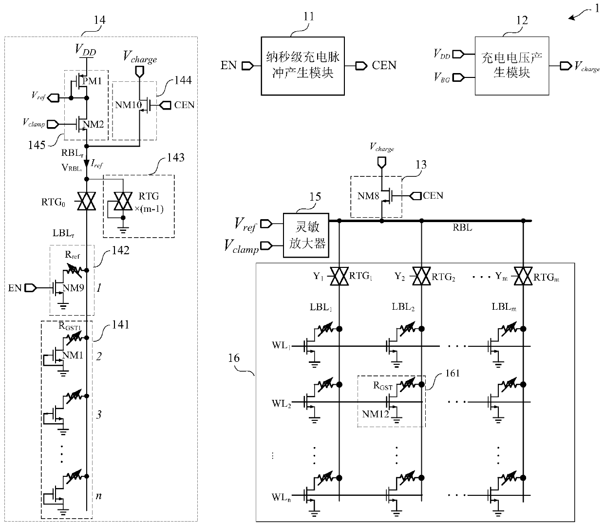
[0090] Such as figure 2 As shown, the present embodiment provides a non-volatile memory readout circuit 1, and the non-volatile memory readout circuit 1 includes: a nanosecond charge pulse generating module 11, a charging voltage generating module 12, and a bit line charging module 13. A first reference read voltage generating circuit 14 and a sense amplifier 15.
[0091] Such as figure 2 As shown, the nanosecond charging pulse generation module 11 receives the read enable signal EN, and generates a post-charge pulse signal CEN after the read enable signal EN arrives.
[0092] Specifically, in this embodiment, the sustaining time of the post-charging pulse signal CEN is set to 100 ps-10 ns. In actual use, the sustaining time of the post-charging pulse signal CEN can be set according to circuit performance and needs. It is not limited to this embodiment.
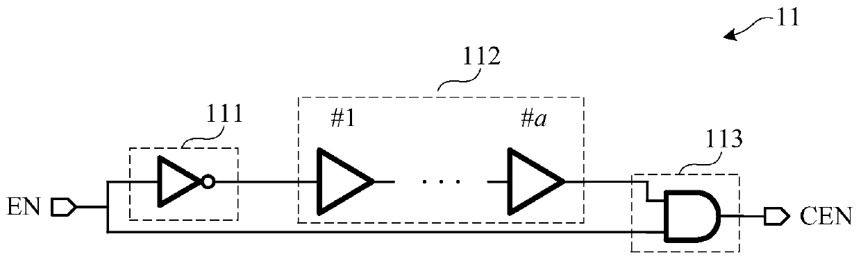
[0093] Specifically, such as image 3 As shown, in this embodiment, the nanosecond charging pulse generation module 1...
Embodiment 2
[0124] Such as Figure 2 ~ Figure 6 As shown, this embodiment provides a method for reading out a non-volatile memory, and the method for reading out a non-volatile memory includes:
[0125] After the read enable signal EN is valid, the read operation starts, a word line and a bit line are selected, and a post-charging pulse signal CEN is generated at the same time.
[0126] At the same time when the read enable signal EN is valid, the read current Vread of a selected memory cell in the memory array 16 is read.
[0127] At the same moment when the read enable signal EN is valid, the read bit line is charged based on the post charge pulse signal CEN.
[0128] At the same moment when the read enable signal EN is effective, the reference read bit line is charged based on the post-charge pulse signal CEN to generate a dynamic reference read current Iref, and the reference read current Iref is the same as the read current Iread The transient curves of the reference read current I...
PUM
Abstract
The invention provides a non-volatile memory reading circuit and a non-volatile memory reading method, and the circuit comprises a nanosecond-level charging pulse generation module which generates a post-charging pulse signal; a charging voltage generation module which generates a post-charging voltage; a bit line reading charging module which is used for charging a bit line to be read; a first reference read voltage generation circuit which charges the reference read bit line and generates a reference read current and a first reference read voltage; and a sense amplifier which is used for comparing the reference read current with the read current to generate a read voltage signal. According to the invention, the rising speed of the reading bit line voltage is improved, the peak value of the reading current is reduced, the dynamic power consumption is reduced, and the time required for the reading current and the reference reading current to reach stable values is reduced; and matching of parasitic parameters is introduced into the reference reading current, matching of parasitic parameters of the current mirror is introduced into the reading current, and post-charging operation is carried out on the reading bit line and the reading reference bit line, so that the pseudo reading phenomenon is eliminated to the maximum extent, and the reading time is reduced.
Description
technical field [0001] The invention relates to the technical field of integrated circuits, in particular to a nonvolatile memory readout circuit and a readout method. Background technique [0002] In the field of integrated circuit manufacturing, as the process nodes continue to shrink, traditional charge-based memories are increasingly limited. Various new memories and new structures have been invented to break through the original limits: MLC NAND, MLC NOR, TLC NAND, MRAM, RRAM, FeRAM, 3D-Xpoint, 3D-NAND, etc. The read latency of traditional and new memories is different: for SRAM as memory, the read time of DRAM is within 10ns, that of NAND Flash is around 50us, that of 3D-NAND is around 500us, and that of hard disk is around 10ms. If the read time of the memory can be further mined, its competitiveness will be greatly improved. [0003] Phase Change Memory (Phase Change Memory, PCM) is a memory based on the Ovshinsky electronic effect proposed by Ovshinsky in the late...
Claims
Application Information
Patent Timeline
Application Date:The date an application was filed.
Publication Date:The date a patent or application was officially published.
First Publication Date:The earliest publication date of a patent with the same application number.
Issue Date:Publication date of the patent grant document.
PCT Entry Date:The Entry date of PCT National Phase.
Estimated Expiry Date:The statutory expiry date of a patent right according to the Patent Law, and it is the longest term of protection that the patent right can achieve without the termination of the patent right due to other reasons(Term extension factor has been taken into account ).
Invalid Date:Actual expiry date is based on effective date or publication date of legal transaction data of invalid patent.
Patent Type & Authority Applications(China)
IPC IPC(8): G11C16/24G11C16/26
CPCG11C16/24G11C16/26
Inventor 雷宇陈后鹏宋志棠
Owner SHANGHAI INST OF MICROSYSTEM & INFORMATION TECH CHINESE ACAD OF SCI