Power semiconductor device comprising metal plate and substrate arranged on the metal plate

A technology of power semiconductors and metal plates, which is applied in semiconductor devices, semiconductor/solid-state device components, electric solid-state devices, etc., can solve problems such as high heat load, cracks in ceramic plates, etc., and achieve efficient cooling and good thermal connection effects

Pending Publication Date: 2019-09-24
SEMIKRON ELECTRONICS GMBH & CO KG
View PDF2 Cites 0 Cited by
  • Summary
  • Abstract
  • Description
  • Claims
  • Application Information

AI Technical Summary

Problems solved by technology

The disadvantage in this case is that during the production of the connection of the base plate to the base plate, the entire arrangement is subjected to a high thermal load by soldering or sintering the layers, and in the case of the sintering layer, even additionally to a considerable pressure load, which Can cause cracks in ceramic plates

Method used


Image

  • Power semiconductor device comprising metal plate and substrate arranged on the metal plate
  • Power semiconductor device comprising metal plate and substrate arranged on the metal plate
  • Power semiconductor device comprising metal plate and substrate arranged on the metal plate

Examples


Embodiment Construction

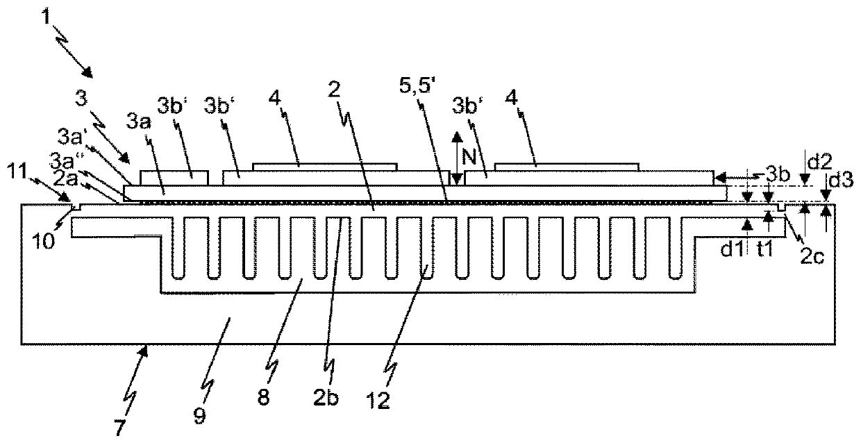
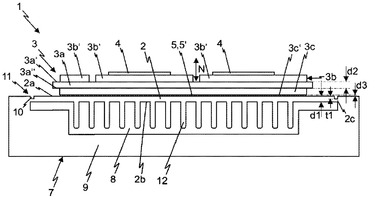
[0032] figure 1 A cross-sectional view of an embodiment of the power semiconductor device according to the present invention is shown. figure 2 Showing a cross-sectional view of another embodiment of a power semiconductor device according to the present invention,

[0033] The corresponding power semiconductor device 1 according to the present invention has a metal plate 2 and a substrate 3 arranged on the metal plate 2. The base plate 3 has a ceramic plate 3a, and a first main side 3a' of the ceramic plate 3a facing away from the metal plate 2 is coated with a first metallization layer 3b configured to form a conductor track 3b'. The conductor tracks 3b' are arranged on the ceramic plate 3a at a distance from each other. The conductor tracks 3b' are arranged on the ceramic plate 3a in a manner electrically insulated from each other. For example, the substrate 3 can be formed as a direct copper-bonded substrate (DCB substrate) or as an active metal brazing substrate (AMB substr...


PUM

PropertyMeasurementUnit
thicknessaaaaaaaaaa
thicknessaaaaaaaaaa

Abstract

The present invention relates to a power semiconductor device (1) comprising a metal plate and a substrate arranged on the metal plate, comprising: a metal plate (2); a substrate (3) arranged on the metal plate (2) and having a ceramic plate (3a), a first main side (3a') of the ceramic plate (3a) facing away from the metal plate (2) being coated with a first metallization layer (3b), which is designed to form a conductor track (3b'); a power semiconductor component (4) which is arranged on the conductor track (3b') and is electrically conductively connected to the conductor track (3b'); and an adhesive (5) arranged between the metal plate (2) and the substrate (3), the adhesive (5) having respective mechanical contact with the first main side (3a'', 3c') of the substrate (3) and the first main side (2a) of the metal plate (2), and forming an adhesive bonded connection connecting the substrate (3) to the metal plate (2) in a material bonded manner.

Description

Technical field [0001] The present invention relates to a power semiconductor device including a metal plate and including a substrate arranged on the metal plate. Background technique [0002] DE 10 2016 104 283 A1 discloses a power semiconductor device that includes a metal plate and includes a base plate arranged on the metal plate, wherein the base plate has a ceramic plate and is bonded to the base plate in a material bonding manner by welding or sintering layers. The disadvantage in this case is that during the manufacture of the connection between the base plate and the bottom plate, the entire arrangement is subjected to a relatively high thermal load by welding or sintering the layer, and in the case of the sintering layer, it is even additionally subjected to a considerable pressure load. Can cause cracks in the ceramic plate. [0003] DE 10 2016 205 178 A1 discloses a substrate which is bonded to a heat sink by means of an adhesive in a material bonding manner. Summary...

Claims


Application Information

Patent Timeline
Patent Type & Authority Applications(China)
IPC IPC(8): H01L23/373H01L23/473
CPCH01L23/3735H01L23/473H01L23/3677H01L23/3672H01L23/13H01L23/36H01L2224/32225H01L2224/48227H01L2224/73265H01L2224/8384H01L2224/291H01L2924/13091H01L2924/13055H01L2924/1301H01L24/32H01L25/072H01L2224/83815H01L25/18H01L2924/00012H01L2924/014H01L2924/00014
Inventor 约尔格·阿蒙哈拉尔德·科波拉
Owner SEMIKRON ELECTRONICS GMBH & CO KG
Why Eureka
Try Eureka