Voltage sag reason identification method and system
A voltage sag and recognition method technology, which is applied in character and pattern recognition, pattern recognition in signals, instruments, etc., can solve the problems of poor real-time performance and low recognition accuracy of voltage sag causes, and reduce the calculation scale and provide real-time The effects of improved performance and recognition accuracy
- Summary
- Abstract
- Description
- Claims
- Application Information
AI Technical Summary
Problems solved by technology
Method used
Image
Examples
Embodiment 1
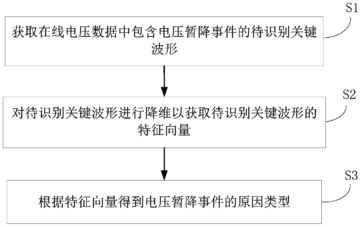
[0027] An embodiment of the present invention provides a method for identifying the cause of a voltage sag, such as figure 1 As shown, the method includes the following steps:
[0028] Step S1: Obtain key waveforms to be identified that include voltage sag events in the online voltage data.
[0029] In the embodiment of the present invention, the sag waveform of online data is captured within a preset time window (for example, a time window of 1 min), and the waveform data with the deepest sag depth is selected as the key waveform.
[0030] Step S2: Dimensionality reduction is performed on the key waveform to be identified to obtain the feature vector of the key waveform to be identified.
[0031] In the embodiment of the present invention, the number of sampling points in the power quality monitoring terminal is 128, and the power frequency is 50hz, so the number of data points in 1 minute is 384,000, and the data dimension of the key waveform to be identified is relatively ...
Embodiment 2
[0068] An embodiment of the present invention provides a voltage sag cause identification system, such as Figure 6 As shown, the system includes:
[0069] The key waveform acquisition module 1 to be identified is used to acquire key waveforms to be identified including voltage sag events in the online voltage data; this module executes the method described in step S1 in Embodiment 1, which will not be repeated here.
[0070] The feature vector acquisition module 2 is used to reduce the dimensionality of the key waveform to be identified to obtain the feature vector of the key waveform to be identified; this module executes the method described in step S2 in Embodiment 1, which will not be repeated here .
[0071] The cause type obtaining module 3 is configured to obtain the cause type of the voltage sag event according to the feature vector. This module executes the method described in step S3 in Embodiment 1, which will not be repeated here.
[0072] The voltage sag cause...
Embodiment 3
[0074] An embodiment of the present invention provides a computer device, such as Figure 7 As shown, it includes: at least one processor 401 , such as a CPU (Central Processing Unit, central processing unit), at least one communication interface 403 , memory 404 , and at least one communication bus 402 . Wherein, the communication bus 402 is used to realize connection and communication between these components. Wherein, the communication interface 403 may include a display screen (Display) and a keyboard (Keyboard), and the optional communication interface 403 may also include a standard wired interface and a wireless interface. The memory 404 may be a high-speed RAM memory (Ramdom Access Memory, volatile random access memory), or a non-volatile memory (non-volatile memory), such as at least one disk memory. Optionally, the memory 404 may also be at least one storage device located away from the aforementioned processor 401 . The processor 401 may execute the method for ide...
PUM
 Abstract
Description
Claims
Application Information
 - R&D
- Intellectual Property
- Life Sciences
- Materials
- Tech Scout
- Unparalleled Data Quality
- Higher Quality Content
- 60% Fewer Hallucinations
Browse by: Latest US Patents, China's latest patents, Technical Efficacy Thesaurus, Application Domain, Technology Topic, Popular Technical Reports.
© 2025 PatSnap. All rights reserved.Legal|Privacy policy|Modern Slavery Act Transparency Statement|Sitemap|About US| Contact US: help@patsnap.com


